
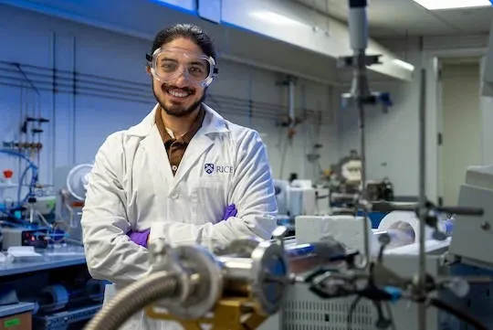
“This is the first demonstration of a transfer-free method to grow 2D devices,” claimed researcher Sathvik Iyengar (pictured). “This is a solid step toward reducing processing temperatures and making a transfer-free 2D semiconductor-integration process possible.”
Serendipity had a hand in the discovery.
“We received a sample from a collaborator that had gold markers patterned on it,” said fellow researcher Lucas Sassi. “During CVD [chemical vapour deposition] growth, the 2D material unexpectedly formed predominantly on the gold surface. This surprising result sparked the idea that by deliberately patterning metal contacts, we might be able to guide the growth of 2D semiconductors directly across them.”
The Rice team optimised the precursor materials to lower the synthesis temperature and demonstrated controlled directional growth, and also that disruptive silicides were not forming from reactions between the metals present and the SiO2 substrate.
“A lot of our work in this project was focused on proving that the materials system is still intact,” said Iyengar. “Seeing what happens at the interface between these materials was a great motivator for the research.”
Contact between the gold and 2D dichalcogenide could be tuned between Schottky and Ohmic behavior by altering deposition thickness.
“Understanding how these 2D semiconductors interact with metals, especially when grown in situ, is really valuable for future device fabrication and scalability,” said the project’s lead engineer Professor Pulickel Ajayan.
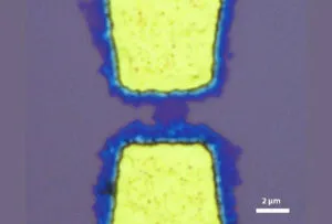
Initially growing on the gold electrodes, the WSe2 was shown to expand across the substrate surface in a stepped fashion, first with many 2D layers, then a few layers and finally as a mono-layer furthest from the electrode.
With growth characteristics understood, the team could then design and deposit a proof-of-concept transistor, with a WSe2 channel between gold electrodes.
Quad Fellowship
Sathvik Iyengar is a fellow of the Japan Society for the Promotion of Science, and an inaugural recipient of the Quad Fellowship, a program launched by the governments of the US, India, Australia and Japan to support early career scientists “in exploring how science, policy and diplomacy intersect on the global stage”, according to Rice.
The project above was sparked by a question raised during a US-India research initiative: Could a semiconductor fabrication process for 2D materials be developed on a limited budget?
“This started through our collaboration with partners in India,” said Iyengar. “It showed how international partnerships can help identify practical constraints and inspire new approaches that work across global research environments.”
The work is described in the paper ‘Mechanistic understanding and demonstration of direct chemical vapor deposition of transition metal dichalcogenides across metal contacts‘, published in ACS Applied Electronic Materials,