
1.Advanced Materials for Enabling Co-Packaged Optics (CPO) Integration.
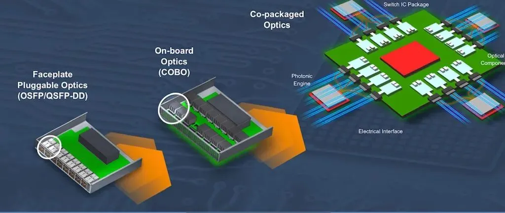
CPO is emerging as a solution to meet computing/communication demands for high bandwidth at low power.
Mark Gerber from ASE gave an overview of the system requirements that are driving CPO material considerations, noting that heat can have significant effects on photonic integrated circuits. He also identified other issues that increase thermal sensitivities in CPO architectures, such as flux outgassing, and described why the order in which assembly steps occur also has an impact.
Rena Huang from RPI said that while much work is taking place to understand and address CPO packaging considerations, much more progress is needed, especially for AI chiplets for large-language models (LLMs), where the key concerns are speed, power and efficiency. She discussed the possibility to build optical networks on optical interposers/wafers/panels, noting that large chiplets could be optically connected with optical interposers, using optical waveguides to reduce loss.
Padraic Morrissey from Tyndall said that for optimum CPO performance, the optics must be moved closer to the edge of compute, and glass has great potential for use as a substrate because it’s optically transparent, has good RF behavior, and lends itself to fabricating high-quality vias. Glass also can work beyond wafers and with really large panels, he said, and can lead to pluggable connectivity. However, he noted that heat is an issue with glass.
Kumar Abhishek Singh from Intel said CPO noted that CPO allows both edge and vertical interconnects, meaning there are many areas where materials come into play. He said that while CPO architectures face unique challenges – such as foreign particles blocking the light path – they also face many of the same issues as non-CPO architectures, such as misalignment and cracks. But these challenges bring opportunities to advance the state-of-the-art.
Christopher Striemer from Aim Photonics described why optically active materials will drive CPO, and also outlined the need for passive material innovations such as 3D printing and novel designs like suspended structures, although right now it’s unclear which ones will offer the most benefit.
2. Hybrid Bonding (HB): to B, or not to B?
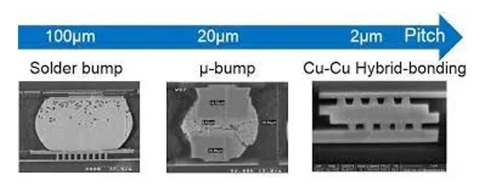
Hybrid bonding is the key technology for high-density 3D integration and advanced packaging, and in recent years, significant advancements were made in pitch scaling, die-to-die bonding, alternative materials, and low-temperature processes. Remaining engineering and technological challenges are defectivity, metrology, design challenges, and cost.
Masha Gorchichko from Applied noted the different types of HB (wafer-wafer, die-wafer, die-die) and said that while HB debuted about 10 years ago in an image sensor from Sony, today the focus is on integrating DRAM memory. She said that advanced metrology is key, because we are now talking about molecular bonds, and therefore an understanding of all the relevant chemical and mechanical requirements is needed. Moreover, to get higher yields and more throughput, not just better but also faster metrology is needed. She noted that thermal concerns are an issue with increasing power density.
Su Jin Ahn from Samsung outlined major HB technology issues and challenges. One is that the many process steps required leave particles on the bonding surface, leading to potential failure. Another is that for AI, the wider, thinner dies used degrade bonding and lead to quality issues. She said what’s needed are advanced metrology/inspection tools and methods, along with design/process co-optimization for bonding. She said the main driver going forward is the need to combine chip and packaging technologies.
Anne Jourdain from imec emphasized the need for fast, reliable metrology solutions, and discussed the pros and cons of copper interconnect and barrier metals.
Chet Lenox from KLA noted the many needs and challenges that come with HB – interposers, warpage control, dielectric interface profiles, clean singulation, bonding alignment – and said that while HB is important, there are other less complex and costly technologies that might preclude the need for HB, such as bridges. He also said that HB creates a need for advanced metrology and inspection capabilities all the way from the front end to packaging.
Laura Mirkarimi from Adeia focused on three areas: metrology improvements for improved throughput and yield; the evolution of 2.5D/3.5D HB packaging technology; and thermal solutions for high power-density chipsets. With regard to metrology, she noted that HB architectural complexity demands a reliable “health of the line” metrology protocol for all process steps. Also, better ways to understand nanoscale topography and to detect surface defects are needed, as are ways to rework HB to reduce costs, such as bond energy engineering. Regarding HB packaging trends and challenges, she said that ultra-high bandwidth, inter-die communication at a 1µm die-to-wafer pitch will require system simplification, such as bonding dies directly to the substrate or using bridge dies to replace an interposer. For thermal management, she described a potential cooling solution that makes use of an integrated manifold and a cold plate bonded to an IC, among other features, and which can be custom-designed to manage specific heat maps.
Masao Tomikawa from Toray said that as the need to bond chips to interposers increases, the need for HB processes that make use of polyimide (PI) resin will become more apparent. That’s because PI enables low-temperature, low-pressure HB processes which minimize warpage and device damage. Many challenges remain, though – precise copper protrusion control and low-temperature copper diffusion bonding are key factors for success.
Brett Wilkerson from AMD spoke from a product perspective. He pointed out that HB requires complex processing. much time and many expensive fab processes, and that it can take several weeks to accomplish, which impacts a company’s time-to-market capabilities. He said thermal resistance is a critical issue, and that there’s a need for standards for the use of HB for memory integration with silicon.
3. Thermal Management Solutions for Backside Power Delivery .
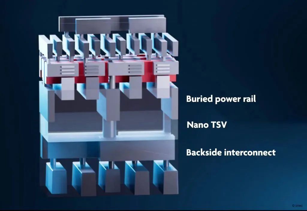
BPD has introduced thermal management challenges and the need for innovative cooling solutions.
Muhannad Bakir from Georgia Tech said that for 3D architectures, interlayer cooling is needed, but asked, how do we enable high-density interconnect within such a structure? He said the solution is to fabricate through-silicon via (TSV) structures with integrated cooling, electrical conductivity, and power, using vertical vias. He addressed the many issues that such a design brings – aspect ratios, TSV heights, etc.
Dureseti Chidambarrao from IBM said that because there are lots of subtleties with BPD architectures, reducing the problem to important basics and solving it with enough accuracy is key. He noted that chip complexity significantly impacts thermal conductivity, and that level-to-level differences can be quite large. He said that an understanding of the entire chip overlay is needed, because there are tricky hot spots, and he described IBM’s strategy, which is to use machine learning plus FEA modeling to calculate the average properties of multiple levels together. He noted that BPD issues only become worse with 3D architectures.
Herman Oprins from imec said it is absolutely critical to identify the basic problems with each particular BPD architecture, because there are so many different flavors of BPD.
Tiwei Wei from Purdue/UCLA said that bond interfaces drive thermal impacts, and she gave an overview of research into different ways to deal with this issue, encompassing factors such as die thickness, CMOS-compatible structures like air gaps or glass bridges, trenches, copper/diamond microbump bonding, two-layer microchannel structures (i.e. manifolds), and others