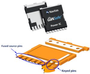
Branded GaNsafe, the company has increased the protection integrated alongside the driver and has moved to 10 x 10mm TOLL packaging, with a custom internal leadframe (diagram below).
The initial products are rated at 650V (800V transients), cover Rds(on) from 35 to 98mΩ (table below), and are aimed at applications from 1 to 22kW. Switching at up to 2MHz is envisaged.
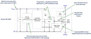
Integrated protection includes short-circuit, over-temperature, under-voltage lock-out, 20V input and 2kV HBM ESD (HBM, 1kV CDM. The short-circuit protection is described both as ’50ns’ and ‘300ns de-saturation’ – only partial details are so far available on the four initial device. They are sampling now, but only to “qualified customers”, said Navitas.
On top of this, on and off dV/dt is now controlled by the driver – set internally in the initial four pin devices, but described as ‘programmable’.
 TOLL package
Surface-mount TOLL packaging has become increasingly popular amongst power semiconductor makers for the package’s low inductance, low electrical resistance and low thermal resistance.
Internally, the leadframe of Navitas’ spin on it has keyed input and Kelvin source pads, but fused main source pads. It passes “IPC-9701 for long mechanical lifetime”, according to the company, referring to ‘IPC-9701 Thermal cycling test method for fatigue life characterization of surface mount attachments’.
Thermal resistance is 0.36K/W, and Navitas claims 100°C junction temperature in an application in which it would reach 112°C in a similar QFN.
| part | Rds(on) 25°C | Id max |
| NV6515 | 35mΩ | 57A |
| NV6513 | 45mΩ | 48A |
| NV6512 | 55mΩ | 34A |
| NV6511 | 98mΩ | 22A |
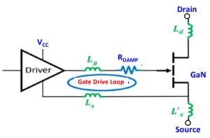
 Integrating the gate driver alongside GaN switching transistors makes a lot of sense as they switch far faster than any other common power transistors – stray driver-to-gate inductance can not only slow them down, but increases the chance of transient damage to the somewhat fragile gates.
Navitas is not the only company integrating gate drivers: some do it monolithically and other by co-packaging a silicon die.
In the Navitas case, it started with GaNfast, which can have current sensing and some level of autonomous protection, and then on to GaNsense devices with autonomous over-current and over-temperature protection, “loss-less” current sensing, 30-100ns short-circuit protection, 800V transient operation and 2kV ESD protection.
“During the on-time of each switching cycle, should the peak current exceed the desired limit, then the internal gate drive will turn the GaN IC off quickly and truncate the on-time period to prevent damage from occurring to the IC,” said the company at the introduction of GaNsense.

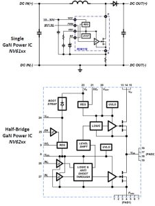
Don’t get too hung up on the brand soup, the features blend from one to the other. Pre-GaNsafe devices (examples left) have also included: on-die regulation, hysteretic inputs, bootstraping, dV/dt control, under-voltage lock-out protection, autonamous stand-by, high-side isolated level-shift, shoot-through protection and a co-packaged silicon low-voltage system controller.
Navitas is fabless, using TSMC to make its GaN die

