
Companies will use the NanoIC line to explore new technologies before they are introduced into large-scale production.
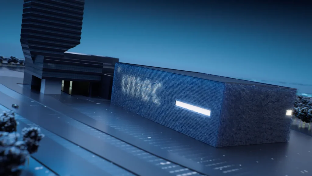
The NanoIC line It will be constructed as an extension (artist’s impression pictured below) of the already existing imec pilot line facilities, built up over the previous decades.
The expected investment of €2.5 billion will be brought together through a combination of public and private contributions.
The contribution from EU funding programs (i.e., Horizon Europe and Digital Europe) through the Chips Joint Undertaking (Chips JU) and Flanders, amounts to an indicative total public funding of €1.4 billion.<
The grant agreement with the Chips JU is currently ongoing and will be signed later this year. The private contributions will come from several industry partners (including ASML) and is set to amount to €1.1 billion.
“The support from EU, the Flemish government and industry partners will enable us to not only retain our leadership position, but also pivot closer to market demands,” says imec CEO Luc Van den hove (pictured right), “the investment will allow us to double volumes and learning speed, accelerating our innovation pace, strengthening the European chip ecosystem, and driving economic growth in Europe.”
The EU Chips Act deploys few pilot lines to address some key challenges facing Europe’s semiconductor industry, such as bridging the gap from innovation to product or fostering collaboration, and to support technology innovation, economic growth, and strategic autonomy.
As well as hosting the beyond 2nm SoC R&D pilot line, imec will participate in the pilot lines on low power FD-SOI and on heterogeneous system integration.
In line with the Chips Act vision, imec and its partners in the NanoIC pilot line CEA-Leti (France), Fraunhofer-Gesellschaft (Germany), VTT (Finland), CSSNT (Romania) and Tyndall Institute will collaborate with European and global equipment and material suppliers to set up the beyond-2nm line.
Additionally, the NanoIC pilot line will play a crucial ‘translator’ role between breakthrough semiconductor innovation and the European industry, enabling companies to explore the most advanced chip technology solutions for their future applications.
With the pilot line, imec aims to lower this threshold by offering early-stage PDKs.
Start-ups, SMEs, universities, and design and system companies can use design pathfinding PDKs for virtual device prototyping, and system exploration PDKs for prototyping of advanced technology components on top of commercially available foundry wafer.
Foundries and IDMs can evaluate innovations in process flows and equipment, allowing for de-risking new features before making internal investments and as such improving the speed and efficiency of industrial process development.
This is particularly significant for OEMs in sectors like health and automotive, where the demand for advanced semiconductor solutions is rapidly increasing.
The NanoIC pilot line will support European OEMs to take leadership in upcoming chiplet-based innovation. Through small volume manufacturing, imec provides a pathway for companies to scale up from prototype to production, once again facilitating rapid innovation and commercialization in the European semiconductor industry.
Key to the pilot line’s success will be the development of a pan-European design platform together with access to a network of competence centers offering training and support to boost design skills.
The design infrastructure will be a critical link between the technology and design communities to accelerate development and reduce time-to-market for new products based on advanced technologies.