
“The results confirm the long-predicted resolution capability of High NA EUV lithography, targeting sub 20nm pitch metal layers in one single exposure,” says Imec CEO Luc Van den hove, “high NA EUV will therefore be highly instrumental to continue the dimensional scaling of logic and memory technologies, one of the key pillars to push the roadmaps deep into the ‘angstrom era’. These early demonstrations were only possible thanks to the set-up of the joint ASML-imec lab allowing our partners to accelerate the introduction of High NA lithography into manufacturing.”.
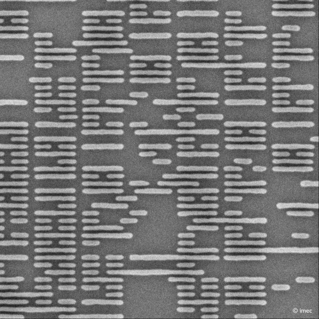
The single exposure random logic structures with 9,5nm dense metal lines, correspond to a 19nm pitch, achieving sub 20nm tip-to-tip dimensions.
Random vias with a 30nm center-to-center distance showcased excellent pattern fidelity and critical dimension uniformity.
2D features at a P22nm pitch exhibited outstanding performance, highlighting the potential of High NA Lithography to enable 2D routing.
“The results showcase the unique potential for High NA EUV to enable single-print imaging of aggressively-scaled 2D features, improving design flexibility as well as reducing patterning cost and complexity,” says imec svp Steven Scheer.
Beyond logic structures, imec successfully patterned, in a single exposure, designs that integrate the storage node landing pad with the bit line periphery for DRAM. This achievement underscores the potential of High NA technology to replace the need of several mask layers by 1 single exposure.
These breakthrough results follow intensive preparatory work by imec and ASML – in close collaboration with its partners – to ready the patterning ecosystem and metrology for the first generation of High NA EUV Lithography.
Prior to the exposures, imec prepared dedicated wafer stacks (including advanced resists, underlayers and photomasks), and transferred High NA EUV baseline processes (such as optical proximity correction (OPC), integrated patterning and etch techniques) to the 0.55NA EUV scanner.