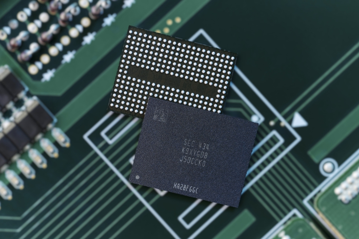
Density is 28.5 Gb/mm² – claimed to be 86% higher than its previous generation QLC V-NAND, with 20% higher data retention performance, double the write performance and 60% faster data input and output speed.

The maximum data transfer rate is 3.2 Gbps.
Data read and write power consumption are said to have been reduced by about 30% and 50%, respectively.
Samsung used channel hole etching technology in a double-stack structure.
Samsung is said to be set to unveil 430-layer NAND chips by the end of 2025.
