
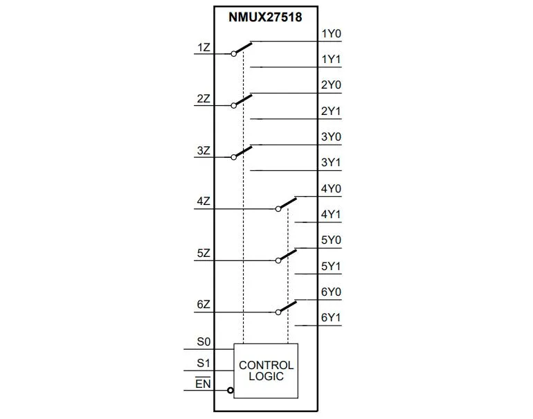
Inside the part, called NMUX27518 (or NMUX27518-Q100 for the automotive version), there are six change-over switches controlled as two blocks of three by two control pads, plus an over-riding chip enable.
The switches can operate with signals anywhere in the 0V to Vcc range.
Off-state cross-talk is typically -58dB, and typical on-resistance is between 8 and 31Ω depending on supply voltage.
Control inputs are compatible with 1.8V logic signals (and backward-compatible with 2.5 and 3.3V logic) even when the device is powered from 3.3V.
“Operating control pins at a lower voltage than the device operating voltage will increase the device supply current,” pointed out the company. Max supply current is usually ~1μA with static inputs (~4nA typ), rising by a maximum of 9μA for each of the three control inputs that are held at 1.8V if the supply is 3.3V.
If power is removed from the IC, all of the control inputs and signal input-outputs become high-impedance to avoid loading surrounding and analogue circuits – as part of this, input and input-output ESD diodes to not have a connection to Vcc. JESD 78 Class II latch-up performance is >100mA.
Operation is across -40 to +125°C, and there are two package options: 4.4mm wide 24pad TSSOP or a 4 x 4mm thermally-enhanced 24 pad QFN 24.
The company sees different roles for AEC-Q100 grade 1 automotive version and the standard version.
It envisages -100 (automotive) types switching quad-SPI bus digital signals between two memories in safety-critical vehicle control units, such as for driver assistance or telematics.
Conversely, it expects the standard IC to route audio and video signals in notebooks, tablets, motherboards and rack servers.
For faster signals, Toshiba has a 26.2GHz (to -3dB) four-channel 2:1 bi-directional multiplexer.