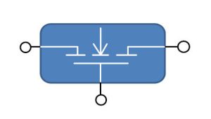
 Innoscience has released an improved bi-directional GaN transistor that can replace back-to-back silicon mosfets in high-side switching.
Called INN040W048A, it is a 40V bi-directional GaN-on-silicon HEMT with on-state resistance as low as 4.8mΩ, which comes in a 2.1 x 2.1mm WLCSP package. It follows on from the 40V 15A 7.8mΩmax (5.5mΩ typ) 2 x 2mm INN40W08, which was never generally released.
“Thanks to the fact that it does not have parasitic diodes, one bidirectional HEMT can be used to replace back-to-back connected nmos mosfets in a common-source configuration to achieve bi-directional switching of the battery’s charging and discharging currents,” according to the company.
Nominally, the device has a gate, two drains and no source.
Electronics Weekly asked how it should be used, and Innoscience said:
The two drain terminals are interchangeable and the gate voltage is refered to one or other drain.
When drain1 or drain2 is positive and the gate is negative, the depletion region extends towards the higher voltage drain side.
When the gate is positive and drain1 or drain2 is negative), the device is turned on and current flows based on the voltage applied on drain 1 and drain 2.Drain-to-drain rating is similar to the drain-to-source voltage rating in a single direction in normal devices. The only difference is that the two drain terminals are interchangeable and the device can block voltage from drain1 to drain2 or from drain2 to drain1.
To turn on the device, the gate voltage needs to be at least 1.7V above drain1 or drain2. To turn off and block current in both directions, gate to drain voltages Vgd1 and Vgd2 need to be below the threshold voltage. A simple way is to pull the gate to ground to turn off the BiGaN.
Existing drivers for back-to-back silicon mosfets can be used, which simplifies the design, if the driving voltage is 5V maximum.
Many applications already use 5V gate driver IC, and for those that uses a 10V max driver, a simple clamped circuit to clamp the gate voltage below 6V is required.
To put this simply: any driver used, is going to have to be the sort used for n-channel high-side switches, with an output voltage above the most positive line in the switched circuit.
Can we see an application note?
Since we are the first in offering bidirectional technology, we are going step-by-step in sharing information in public. We have an application note that is today shared with customers under NDA, and we are working on a public version that will follow soon.
Use is foreseen in over-voltage protection circuits for smartphone charging, high-side load switching, and multi-rail switching – for example in laptop buck-boost chargers with multiple inputs. Phone company Oppo has already adopted a bidirectional GaN switch from Innnoscience inside handsets for direct charging load switching.
In the pipeline are lower on-resistance bidirectional hemts as well as higher voltage types.
There appears to be a INN040W048A data sheet here
