
Analog-to-digital converters (ADCs) have many specifications. Depending on the application requirements, some of these specifications might be more important than others. The DC specifications, such as offset error, gain error, integral nonlinearity (INL), and differential nonlinearity (DNL), are particularly important in instrumentation applications where the ADC is used to digitize slow-moving signals such as those from strain gauges and temperature sensors.
This article delves into a discussion on the offset and gain error specifications.
ADC Transfer Function
The ideal transfer function for a 3-bit unipolar ADC is shown in Figure 1.
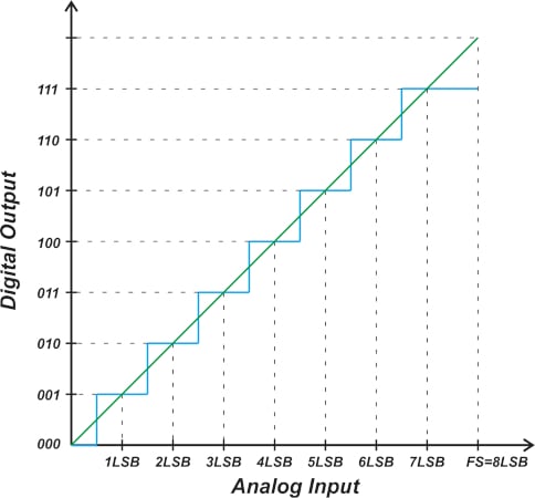
Figure 1. Digital output vs. analog input (transfer function) of a 3-bit unipolar ADC.
Ideally, the ADC exhibits a uniform staircase input-output characteristic. Note that an output code doesn’t correspond to a single analog input value. Instead, each output code represents a small input voltage range equal to one LSB (least significant bit) in width. As shown in the figure above, the first code transition takes place at 0.5 LSB, thereafter each successive transition occurs at 1 LSB from the previous transition. The last transition occurs at 1.5 LSB below the full-scale (FS) value.
Since a finite number of digital codes are used to represent a continuous range of analog values, the ADC exhibits a staircase response, which is inherently nonlinear. When assessing certain non-ideal effects, such as offset error, gain error, and nonlinearity, it is useful to model the ADC transfer function by the straight line that goes through the midpoint of the steps. This line can be expressed by the following equation:
[Y_{Linear}=frac{V_{in}}{FS}times2^{N}]
Where Vin is the input voltage and N denotes the number of bits. If we kept increasing the ADC resolution (or the number of output codes), the staircase response would tend to approach the linear model more and more. Therefore, the straight line can be considered as the transfer function of an ideal ADC with an infinite number of output codes. In practice, however, we know that the ADC resolution is limited and the straight line is only a linear model of the actual response.
ADC Offset Error and the Transfer Function
Due to non-ideal effects like a mismatch between internal components, the actual transfer function of an ADC deviates from the ideal staircase response. The offset error shifts the transfer function along the horizontal axis and hence causes a shift in the code transition points. The purple curve in Figure 2 shows the response of an ADC with +1 LSB offset.
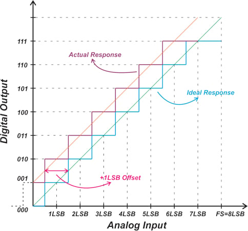
Figure 2. A graph showing the +1 LSB offset, the actual response, and the ideal response.
For a unipolar three-bit ideal ADC, the first transition should occur at 0.5 LSB, changing the output from 000 to 001. However, with the above response, the ADC output transitions from 001 to 010 at 0.5 LSB. The 001 to 010 transition should ideally occur at 1.5 LSB. Therefore, the non-ideal response is shifted by 1 LSB to the left when compared to the ideal characteristic. This is described as +1 LSB offset error. Considering the linear model of the non-ideal response (the orange curve in the figure), we can also observe that the system outputs 001 for a 0V input, corresponding to +1 LSB offset.
Figure 3 shows the response for an ADC with -1.5 LSB of offset error.
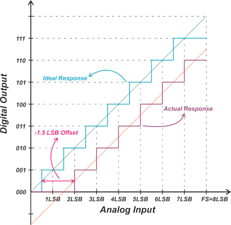
Figure 3. Response of an ADC with -1.5 LSB offset error.
Since the offset error shifts the entire transfer function by the same value, it can easily be calibrated out by subtracting the offset value from the ADC output. To determine the offset error, the first code transition is usually measured and compared with its corresponding transition from the ideal response. Using the first code transition (rather than the next ones) results in a more accurate measurement because the offset error by definition refers to the deviation from the ideal response at zero volts input.
Finding the ADC Offset Error Example
Consider a 10-bit ADC with a full-scale value of FS = 5 V. If the transition from the all-zeros output code to 00…01 occurs at an input voltage of 8 mV, what is the offset error of the ADC?
For a 10-bit ADC with FS = 5 V, the LSB value is 4.88 mV as calculated below:
[LSB=frac{FS}{2^{N}}=frac{5}{2^{10}}=4.88,mV]
While the first transition should ideally occur at 0.5 LSB = 2.44 mV, the measured response makes this transition at 8 mV. Therefore, the ADC has an offset value of -5.56 mV. The offset error can also be expressed as multiples of LSB as follows:
[Offset,Error,(in,LSB)=frac{Offset,Error,(in, Volts)}{LSB,Value,(in, Volts)}=frac{-5.56,mV}{4.88,mV}=-1.14,LSB]
ADC Gain Error
With the offset error eliminated, the first transition of the actual response coincides with that of the ideal characteristic. However, this doesn’t guarantee that the other transitions for the two characteristic curves will also occur at the same input values. The gain error specifies the deviation of the last transition from the ideal value. Figure 4 illustrates the gain error concept.
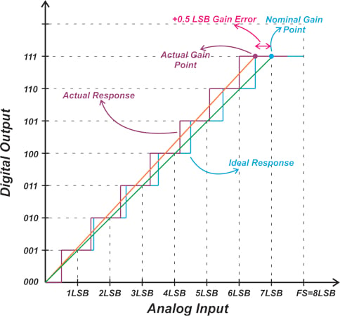
Figure 4. A graph showing the concept of gain error.
Let’s define half LSB above the last transition as the “gain point.” With the offset error eliminated, the difference between the ideal gain point and the actual gain point determines the gain error.
In the above example, the non-ideal characteristic has a gain error of +0.5 LSB. The orange curve in the above figure is the linear model of the non-ideal response. As you can see, a difference between the measured gain point and the ideal gain point actually changes the slope of the linear model of the system. Figure 5 shows the response for an ADC with -1 LSB gain error.
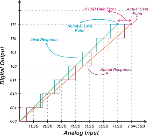
Figure 5. The response for an ADC with -1 LSB gain error.
Note that some technical documents define the gain error as the vertical difference between the actual gain point and the straight line model of the ideal ADC. In this case, continuing with the example depicted in Figure 5, we obtain the diagram in Figure 6.
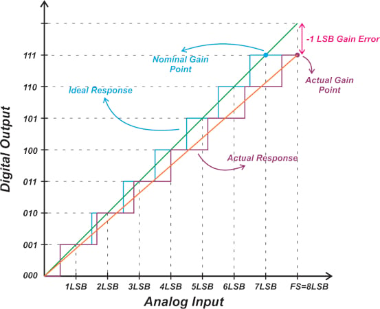
Figure 6. Gain error as the vertical difference between the actual gain point and the straight line model of an ADC.
Both the vertical and horizontal differences yield the same result because the ideal linear model has a slope of one.
Finding the ADC Gain Error Example
Assume that a 10-bit ADC with a full-scale value of FS = 5 V makes its last transition from the hexadecimal value of 3FE to 3FF at 4.995 V. Assuming that the offset error is zero, calculate the ADC gain error.
The LSB of the ADC is 4.88 mV, as calculated in the previous example. The last transition should ideally occur at FS -1.5 LSB = 4992.68 mV. The measured value at which the transition occurs is 4995 mV. Therefore, the ADC has a gain error of -2.32 mV or -0.48 LSB.
Expressing Gain Error in Terms of Full-Scale Error
Building on the concepts discussed above, we can define the gain error in terms of the full-scale error. This is illustrated in Figure 7.
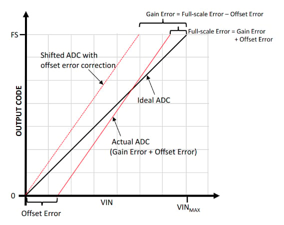
Figure 7. Full-scale error. Image used courtesy of Microchip
In the above figure, the actual response is affected by both offset and gain errors. Therefore, the deviation of the actual last transition from the ideal last transition, which is denoted by full-scale error, contains both offset and gain errors. To find the gain error, we can subtract the offset error from the full-scale error:
[Gain Error,=,Full scale Error,-,Offset Error]
This is equivalent to first compensating for the offset error and then measuring the deviation of the last transition from the ideal response to arrive at the gain error. Note that in this particular example, the gain error is positive and the offset error is negative, leading to a full-scale error smaller than the gain error.
Some ADC Specification Inconsistencies in Definition
It is worth mentioning that some ADC specifications are not consistently defined in technical literature. One confusing inconsistency is the sign of the offset and gain error. For example, while Microchip and Maxim Integrated are consistent with the definitions used in this article, some manufacturers, such as STMicroelectronics (ST), differ. ST defines the sign of these error terms in the opposite way. Inconsistencies are also observed between documents from the same chip manufacturers. For example, Figure 8 is taken from this Texas Instruments (TI) document that uses the opposite sign convention.
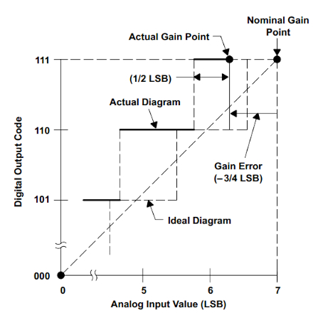
Figure 8. TI’s example for ADC gain errors. Image used courtesy of TI
However, Figure 9, again from TI, uses definitions consistent with those used in this article.
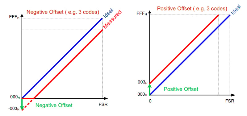
Figure 9. An example of offset error from TI. Image (adapted) used courtesy of TI
The sign convention used in Figure 9 (and throughout this article) seems to be more widely accepted in various technical literature. Despite this. such inconsistencies can cause confusion, though you can get around the problem if you’ve grasped the basic concepts discussed in this article. For example, if you measure an ADC and observe that its first transition occurs above 0.5 LSB (similar to the case depicted in Figure 3), you know that an appropriate positive value should be added to the ADC reading to compensate for the offset error, regardless of the sign convention you are using.
To see a complete list of my articles, please visit this page.