
Called LT8418, this IC looks very much like the output stage used within the recently announced GaN driving dc-dc controller ICs LTC7890 and LTC7891.
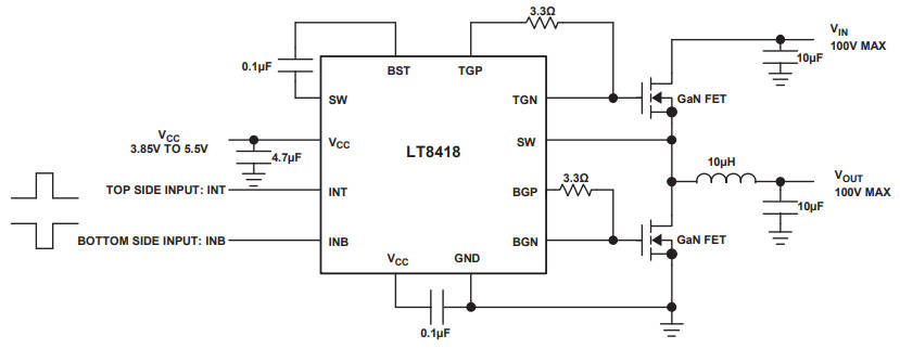
Both high-side and low-side outputs have separate pull-up and pull-down connections on the IC package channels so that additional resistors can be used to tune GaN transistor turn-on and turn-off times separately.
“Split gate drivers allows the customer to adapt the on-off behaviour to address flexible and control issues,” said ADI at the LT8418’s launch at APEC in California.
For both high-side and low-side drive, output current sourcing is via a 0.6Ω pull-up (4A peak), while sinking is through 0.2Ω (8A peak).
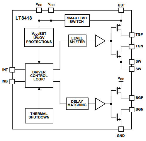
As GaN gates are so sensitive to over-voltage – damage is caused not far above the recommended drive voltage – the high-side bootstrap is not via a conventional diode, but is though a ‘smart-switch’.
During the dead time interval between top-gate turn-off to bottom-gate turn-on, or between bottom-gate turn-off to top-gate turn-on, the GaN power switch demonstrates a reverse conduction voltage of 2 to 3V from source to drain – even higher at high current – which can bring the switch node down to -2 to -3V, and lead to the over-charge of bootstrap rail, and permanent gate damage to the GaN power switch.
The smart bootstrap switch consists of power switches that can fully control bootstrap charging or blocking.
When the bottom switch is turned on and the switching node voltage is close to ground level, the bootstrap switch is turned on to start charging the bootstrap capacitor.
 The bootstrap switch has a typical on-resistance of 6Ω, dropping 0.6V when 100mA is flowing into the bootstrap capacitor. At 100µA, drop is typically 1mV (10mVmax).
Bootstrap under-voltage lock-out protection is included to prevent the GaN transistors turning on with insufficient drive voltage, tripping at 3.1V and clearing at 3.35V (250mV hysteresis).
 The tiny package, a 1.7 x 1.7mm WLCSP BGA, has two internally connected pads for the high-side output. One is intended to provide a low-inductance path to the bootstrap capacitor (see diagram).
The Vcc pin is also doubled, one for the power rail and one for the IC’s decoupling capacitor.
There are two inputs pins, one for the high-side GaN pwm waveform and another for the low-side.
Typically, the input switching threshold is 1.9V with 400mV of hysteresis, and these inputs can tolerate up to 15V (abs max) to allow a variety of signal sources to be used. Each input has an internal 200kΩ pull-down resistor to turn both outputs off if no input signals are present.
No anti-over-lap protection is provided, so if both inputs are set to logic ‘1’ then both GaN output transistors will be turned on simultaneously causing high current flow. “Careful consideration must be applied to the input interface to avoid a possible shoot-through condition,” said ADI.
Regarding applications, ADI said: “LT8418 can be configured into synchronous half-bridge, full-bridge topologies, or buck, boost and buck-boost topologies.”
Find the LT8418 product page here
EPC has used the LTC7891 controller IC mentioned above in this dc-dc demo board