
The Equipment and Process Innovation and Commercialization (EPIC) Center is planned as the heart of an innovation platform designed to accelerate development and commercialisation of the foundational technologies needed by the a semiconductor and computing industries.
To be located at an Applied campus in Silicon Valley, the multibillion-dollar facility is designed to provide a breadth and scale of capabilities that is unique in the industry, including more than 180,000 square feet – more than three American football fields – of state-of-the-art cleanroom for collaborative innovation with chipmakers, universities and ecosystem partners.
Up to $4 billion could be spent on the centre depending on the amount of government funding it can attract.
Designed from the ground up to accelerate the pace of introducing new manufacturing innovations, the new EPIC Center is expected to reduce the time it takes the industry to bring a technology from concept to commercialization by several years, while simultaneously increasing the commercial success rate of new innovations and the return on R&D investments for the entire semiconductor ecosystem.
“This investment presents a golden opportunity to re-engineer the way the global industry collaborates to deliver the foundational semiconductor process and manufacturing technologies needed to sustain rapid improvements in energy-efficient, high-performance computing,” says Applied CEO Gary Dickerson.
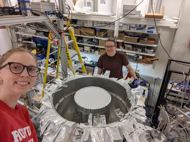
The complexity of the engineering challenges requires a new approach to R&D. The traditional development model, starting with materials engineering equipment and process innovation, is a serial, compartmentalized process with no central hub for collaboration across the ecosystem.
The industry needs a new model that breaks down traditional silos, builds denser networks of collaboration, and delivers tighter feedback loops that can increase the speed and lower the cost of innovation.
Applied’s new EPIC Center is designed to be a premier platform for leading logic and memory chipmakers to collaborate with the equipment ecosystem. For the first time, chipmakers can have their own dedicated space within an equipment supplier facility, extending their in-house pilot lines and providing early access to next-generation technologies and tools – months or even years before equivalent capabilities can be installed at their facilities.
A number of leading semiconductor and computing companies, including AMD, IBM, Intel, Micron, Nvidia, Samsung, TSMC and Western Digital, have commented on today’s announcement. The videos are available here.
The platform is also expected to be a catalyst for accelerating the commercialization of academic research and strengthening the pipeline of future semiconductor industry talent.
Universities are uniquely skilled at ideating new concepts, but they often lack access to state-of-the-art industrial labs and hardware which can impede their ability to turn ideas into commercial reality. Applied’s new platform can provide university researchers access to the full range of industrial-scale capabilities to validate their ideas, increasing the success rate of innovations and reducing the time and cost of commercializing new technologies.
This would be achieved with a two-pronged approach. University researchers can perform research alongside industry professionals in the new EPIC Center, and Applied can collaborate with academic partners to build a network of industrial-quality satellite labs at university facilities.
The new approach is designed to build upon Applied’s existing relationships with top engineering schools, such as Arizona State University, where Applied has been conducting research in materials science and semiconductor technology alongside faculty and students