
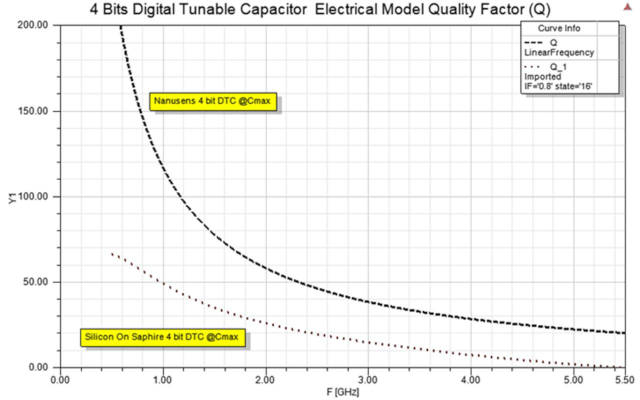
The Q-factor is above 100 at 1GHz, and the four-bit capacitor has a minimum capacitance of 450fF (30fF/capacitor) with them all off and tunes up to ~1pF – a capacitance ratio of 2.2 which the company expects to extend to 4 in the next version. Linearity >90dBc for IMD3.
 A single 30-66fF switchable capacitor
“This solves the low Q factor problem as there is no on-state resistance,” according to the company. “The RF mems issues of dielectric charging and breakdown do not exist as no dielectric is used in this design. This results in superior reliability.”
The moving parts are flat plates, suspended by meandering springs, which are moved sideways (in the plane of the IC, not up-and-down) by electrostatic force to vary the capacitance.
Over four billion switching cycles have been demonstrated without degradation in the lab, said Nanusens, and the devices have been tested for shock, vibration and thermal cycling tolerance, as well as moisture sensitivity (MSL 1) and HTSL (high-temperature storage life).
The integrated capacitors are being pitched for antenna tuning in phones.
 “We have test chips for upper 5G bands with customers and they actually advised us to use this technology to also create solutions for 6G as the industry really has a challenge,” said Nanusens CEO Josep Montanyà. “The issue is that 6G needs to be able to handle many more, and possibly higher, frequencies than 5G. To do this requires additional antennas to be integrated into the phone to handle more bands but, due to them having to be smaller to fit more of them inside the phone, their efficiency decreases. In order to get the best possible performance from each antenna, each needs to be tuned to reconfigure to different bands and to avoid mismatch with the power amplifier. This is currently done by means of tunable capacitors.”
The company’s intellectual property covers building mems structures – masses, springs and switches – built within the metal layers formed during back-end-of-the-line (BEOL) semiconductor processing, allowing them to sit above power amplifiers and LNAs in the silicon below.
Only standard CMOS processes “with minimal post-processing” is needed (inter-metal dielectric is etched away through the pad openings in the passivation layer using vapour HF, with the holes sealed before packaging), and die remain compatible with WLCSP packages, it added.
Founded in 2014, Nanusens is headquartered in Devon, England, with R&D in Barcelona and Shenzen. It is built on technology from the founders’ previous company Baolab Microsystems, and has venture funding from Inveready, Caixa Capital Risc and Dieco Capital.