
 The interfaces in assemblies of 2D materials could produce opto-electronics devices, according to Monash University in Australia, which is designing them using density functional theory (DFT) based band-structure modelling.
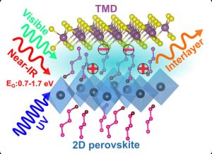
“2D perovskites show interesting photo-physical properties and better stability compared to typical bulk perovskites,” according to Monash. “However, till now, near-infrared and visible-range optoelectronic device performance metrics of 2D perovskites have been quite poor owing to certain intrinsic and materials-specific limitations such as large bandgaps, unusually high exciton binding energies and low optical absorption.”
Key to the research is to conjugate 2D perovskites with optically active transition metal dichalcogenides (TMDs) – although structurally dissimilar, 2D perovskites and TDMs can form clean interfaces through the same inter-layer van der Waals interactions that hold layers of graphene in graphite together.
Supercomputer-based modelling at the university indicates that novel band alignment and transport properties are feasible in 2D perovskite-TMD heterostructures which can be tuned by choosing different lattice-matched materials.
It was found that certain alignments with near-infra-red and visible light bandgaps can enhance optical absorption “at comparatively lower energies”, said Monash. “Also, sizeable band offsets and possibility of interlayer excitons with lower dissociation energies can lead to easier inter-layer separation of the excited charge carriers across two materials.”
The result is higher photo-currents and a chance to improve solar cell efficiencies.
Another prediction is that other inter-material alignments will create light-emitting interactions and yet further alignments will offer tunnelling transport.
An added benefit is that strain tolerance is predicted in such 2D perovskite-TMD heterostructures, making flexible sensors a possibility.
“Overall, these findings demonstrate that a computationally-guided selection of heterostructures could offer better platforms than intrinsic materials for specific device applications, and have potential in next-generation multi-functional devices such as flexible photosensors or LEDs,” said researcher Nikhil Medhekar, who led the work with Abin Varghese and Yuefeng Yin.
Monash University worked with the University of Queensland and the Indian Institute of Technology Bombay.
“Near‐infrared and visible‐range optoelectronics in 2D hybrid perovskite/transition metal dichalcogenide heterostructures” describes the work in Advanced Materials Interfaces. Available in full without payment, this paper describes the different forms of bandgap interactions involved in detail.