
Embedded computing designs often have two dominant demands: low power consumption to extend the lifespan of small batteries and an accurate and reliable interface with sensors that provide information about the surrounding environment. To support these two trends, Renesas recently announced a new family of microcontrollers (MCUs) that combine ultra-low power consumption with high-accuracy analog-to-digital conversion (ADC).
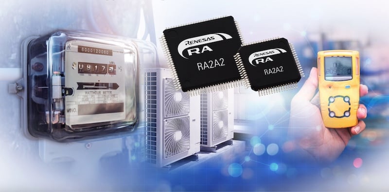
The new RA2A2 microcontrollers. Image used courtesy of Renesas
Let’s take a look at the new MCUs and the theory behind high-accuracy ADCs.
Renesas Introduces RA2A2 MCUs
The Renesas RA2A2 microcontrollers offer a suite of advanced features tailored for applications demanding high-resolution analog capabilities and efficient over-the-air updates.
At their core, these MCUs (datasheet linked) leverage the energy-efficient Arm Cortex-M23 32-bit processor, achieving a balance between processing power and energy consumption with a top operational frequency of 48 MHz. This processor is built on the Armv8-M architecture, complete with integrated functionalities for enhanced security and reliability, such as a single-cycle integer multiplier, a 19-cycle integer divider, and an Arm Memory Protection Unit with eight regions.
Designed with a rich memory architecture, the RA2A2 series offers up to 512 KB of dual-bank code flash memory, facilitating application updates without halting device operation. Additionally, an 8-KB data flash memory supports data storage with high endurance, complemented by 48 KB of SRAM for efficient data handling during runtime operations. Renesas claims that the new devices’ dual-bank code flash and bank swap functions allow designers to implement firmware over-the-air (FOTA) updates for IoT use cases that may benefit from remote updates, including building automation, medical devices, and various consumer electronics.

RA2A2 MCU block diagram. Image used courtesy of Renesas
The connectivity options in RA2A2 MCUs are extensive. They feature five serial communications interface channels, a serial peripheral interface, and two I2C bus interfaces. These interfaces ensure versatile communication capabilities with other integrated circuits, sensors, and peripherals.
One distinguishing characteristic of the RA2A2 series is its analog features, highlighted by a 24-bit Sigma-Delta A/D converter and a 12-bit A/D converter. These converters offer high-precision signal measurement, accommodating diverse sampling rates of 7.813 kHz/8.333 kHz or 3.906 kHz/4.166 kHz for accurate analog-to-digital conversion. Furthermore, the MCUs are engineered for power efficiency with ultra-low power operation as low as 100 µA/MHz in active mode and 0.40µA in software standby mode.
Sampling Rate and ADC Accuracy
Digital signal processing system design requires understanding the relationship between sampling rate and the accuracy of the analog-to-digital converter (ADC).
The sampling rate, defined as the frequency at which an analog signal is sampled to convert into a digital form, plays a pivotal role in capturing the signal’s essence without losing significant information. On the other hand, ADC accuracy, often influenced by noise, determines the precision with which the analog signal is represented in its digital form.
A fundamental principle governing the interaction between sampling rate and ADC accuracy is the Nyquist theorem, which states that the sampling rate must be at least twice the maximum frequency present in the analog signal to accurately reconstruct the signal without aliasing. However, increasing the sampling rate beyond this minimum requirement does not linearly improve the accuracy of the digital representation. In fact, at higher sampling rates, several factors can introduce noise, potentially degrading ADC accuracy.
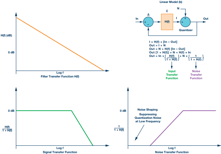
The theory behind sigma-delta ADCs. Image used courtesy of Analog Devices
Higher sampling rates can help decrease the impact of quantization noise, a type of error during the quantization process of converting continuous analog signals into discrete digital numbers. This noise is inherent to the ADC process and is inversely proportional to the ADC’s resolution.
This phenomenon can be better understood through the concept of oversampling, which involves sampling the analog signal at a rate significantly higher than the minimum required by the Nyquist criterion. Oversampling increases the frequency spectrum available for distributing the quantization noise, thereby reducing its density within any given bandwidth. This reduction in noise density translates to an improved signal-to-noise ratio (SNR) within the signal bandwidth, leading to a more accurate representation of the original signal after digital filtering is applied to remove the out-of-band noise.
Oversampling, coupled with noise-shaping techniques such as sigma-delta modulation, can push the quantization noise away from the lower frequencies (where it is most perceptible) to higher frequencies. This enables an even more effective noise reduction within the signal’s bandwidth after digital filtering, further enhancing the ADC’s effective resolution and accuracy.
Features for Modern Embedded Designs
Because modern embedded applications must reliably interface with sensors and consume minimal power, Renesas RA2A2 MCUs meet a major need in the marketplace. With its low power consumption, high-sampling-rate ADCs, and a variety of communication peripherals, the new family may be particularly useful in consumer electronics and IoT devices.