
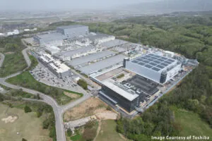
In May, Toshiba officially opened phase 1 of its Kaga wafer fab expansion. The facility in Japan’s Ishikawa Prefecture and brings online 300mm/12-inch wafer lines.
Adrian Cotterill, Farnell’s power segment lead, commented: “Japan holds significant importance for us, and our enhanced partnership with Toshiba reflects our commitment to delivering advanced semiconductor solutions to meet the evolving needs of engineers and designers in the region”.
When Kaga phase 1 reaches full-scale operation, production capacity for power semiconductors (mainly mosfets and IGBTs) will more than double its 2021 capacity.
The Kaga fab has an earthquake absorbing structure. When it was announced, the company said it aims to achieve the RE100 goal of 100% reliance on renewable energy. The fab also uses AI and automated wafer transportation systems for quality and production efficiency.
Farnell Global is an Avnet company. the distributor trades as Newark in the Americas, Farnell in Europe, the Middle East, Africa and Japan, and element14 across Asia Pacific. It also sells direct to consumers through its CPC business in the UK.
Related: