
Scandium aluminum nitride (ScAlN) is a novel material that could make these transistors better as it can increase carrier concentration.
“It exhibits large polarisation, which increases electron densities in the two-dimensional electron gas,” according to the Tokyo University of Science. “Additionally, its ferroelectric nature makes it suitable for use as a ferroelectric gate material in ferroelectric hemts. Such a gate enables dynamic control over the electron gas, offering potential to diversify the functionality of GaN-based devices.”
However, it is not an easy material to grow in a controlled way.
Sputtering can make it, but not at sufficient quality, and molecular beam epitaxy can also succeed, but too slowly for production. This is according to the Fraunhofer Institute for Applied Solid State Physics (IAF) in Germany, which managed to make for the first time using production-friendly MOCVD back in 2019, achieving ~600cm2/V/s mobility and ~4 x 10¹³/cm2 carrier density.
This MOCVD process is now patented, and Fraunhofer IAF along with other institutions reported an electron gas carrier density of 5 x 10¹³/cm2 at the International Conference on Nitride Semiconductors this year.
Tokyo University of Science is talking about ScAlN today because it has revisited sputtering, finding that high temperature is the key to improve sputtered ScAlN thin film epitaxial on AlGaN-AlN-GaN heterostructures.
“Compared to expensive and complex deposition techniques, sputtering, widely used in electronics manufacturing, can enable the mass production of ScAlN thin films at much lower costs, making high-performance devices more accessible,” said Tokyo researcher Atsushi Kobayashi.
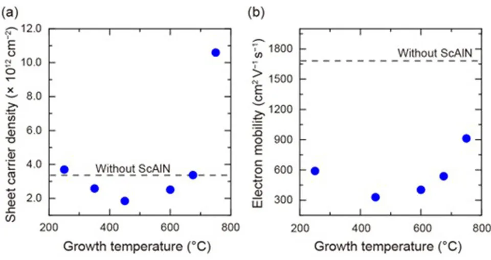
They were 10% scandium films, studied using atomic force microscopy, electron diffraction and Hall-effect measurements.
Surface flatness of the films improved above 250°C and, at 750°C, step-and-terrace features appeared suggesting high structural quality beneath.
Carrier density in the 2-d gas in the sample grown at 750°C reached 1.1 x 10¹³/cm2,” approximately three times that of AlGaN-AlN-GaN heterostructures without ScAlN”, said the university, while films grown at lower temperatures were worse than without ScAlN (see graph).
Electron mobility in the 750°C Tokyo ScAlN-inclusive samples was ~900cm2/V/s, still lower than 1,677cm2/V/s scored by the team’s non-ScAlN reference – attributed by the researchers to roughness and structural imperfections introduced by the ScAlN barrier.
“Our study demonstrates the viability of sputtering for growing high-quality ScAlN layers on GaN, offering a practical path towards the commercialisation of GaN hemts with ScAlN barriers,” said Kobayashi.
The work is published as ‘Effect of growth temperature on the structural and electrical properties of sputter-epitaxial ScAlN on AlGaN/AlN/GaN heterostructures‘ in APL Materials – can be read in full without payment.
Last year, Tokyo Tech turned to scandium for ferroelectric memory materials