
July 11, 2022
Interferometry has been a technique for measuring distance for over a century. By using the interference of sound, light or electromagnetic waves and analyzing the received superimposed waves, users can extrapolate precise distances. Micro-Epsilon accomplishes this level of high precision distance and thickness measurements with an innovative white light interferometer technology. These sensors can obtain absolute measurement distances without the need for a reference, allowing them to maintain a precision measurement value before and after signal interruption. This is a massive advantage for distance control and profile measurements of moving objects.
White light interferometers — Overview
The concept of interferometry has been tried and tested in numerous applications. With this technique, a beam splitter divides a light wave into two partial beams to take different paths. Signal processing techniques can be used to analyze this constructive and destructive interference pattern of the signals to obtain precise measurements of distance and surface properties of the material under test. The light source itself can vary between a laser or a superluminescent diode (SLED or SLD).
White light interferometers with SLDs use an extended wavelength spectrum to obtain more distance information, allowing the sensor to take absolute measurements with no reference required. With this technique, the white light interferometer can obtain more accurate measurements that are absolute and not just relative. This is a critical characteristic for many industrial metrology applications. In contrast to white light interferometers, laser interferometers use highly coherent monochromatic light where the waves are in phase. This allows users to only perform relative measurements with a preset reference.
What Micro-Epsilon has to offer
Micro-Epsilon offers two main types of white light interferometers ― one optimized for absolute distance and the other for thickness measurements. The IMS5600-DS models are designed for high-resolution distance measurements that can also be performed in a vacuum for clean room environments. On the other hand, the IMS5400-TH performs stable thickness measurements. Each of these measurement methodologies will be more optimally suited toward different industrial metrology applications. Table 1 details how these white light interferometers can be used.
 Table 1. Measurements accomplished by absolute distance and stable thickness interferometers.
Exploring industrial metrology use cases with white light interferometers
Applications for absolute distance interferometers
The absolute distance measurement is used for high-precision displacement and distance measurements. The ability to detect absolute measurement values enables the distance measurement of step-height profiles with a high signal stability. Step profiles with heights on the subnanometer-level can be measured with the interferometers that have resolutions on the order of picometers. Measurements can also be made on moving objects with the ability to track the differences in height of heels, as well as steps and depressions.
Subnanometer resolution is often necessary in the semiconductor industry for wafer tilt measurements, wafer stage position and aligning photomasks (Figure 1). In wafer tilt measurements, these interferometers measure the horizontal tilt of wafers as they are fed in, to ensure position accuracy when picked up and removed. Multi-axis, ultra-high precision metrology is also necessary for positioning the wafer stage where the interferometers measure the XYZ movements of the stage with extremely high accelerations. These types of absolute measurements are not exclusive to semiconductor fabrication facilities. This type of optical scanning is leveraged, e.g., for testing the roundness of shafts on a rotating part.
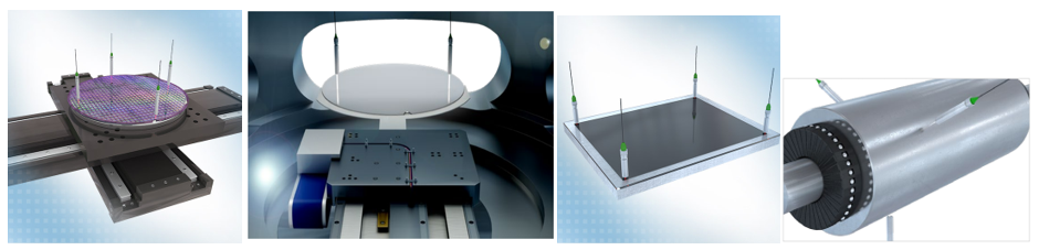 Figure 1. White light interferometers offer picometer-level resolutions, ideal in the semiconductor industry for positioning the wafer stage, wafer tilt measurements, photomask positioning and testing shaft concentricity (left to right). Source: Micro-Epsilon
Another use case is the multi-peak distance measurement that obtains distance values on transparent objects. Up to 14 distance values are simultaneously evaluated in a measuring range of 2.1 millimeters by analyzing signal peaks; from this, a thickness measurement can be extrapolated. This, for instance, can be used to calculate the distance between glass and a carrier plate. From this distance value, the controller can ascertain the thickness of the glass.
Applications for stable thickness interferometer
The stable thickness measurement achieves a nanometer-accurate thickness value even with moving objects and from a relatively large distance. It enables the measurement of extremely thin layers found in flat glass, films and optically non-dense objects such as anti-reflective coated glass (Figure 2). This distance-independent measurement is achieved even with fluttering material during production such as flat plastic film . The target can move within the measuring range without influencing the accuracy of the values obtained.
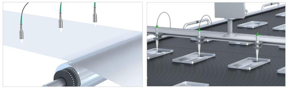 Figure 2. Stable thickness measurements for inline thickness monitoring of plastic films (left) and height measurement of glass inserts (right). Source: Micro-Epsilon
The stable multi-layer thickness measurement yields thickness values of the layers within transparent objects by evaluating several signal peaks simultaneously. Based upon the measurement, up to five thickness values are then outputted by the controller. This is the difference between the stable multi-layer thickness measurement and the multi-peak distance measurement ― the stable thickness measurement will return the thickness values of multiple (up to five) individual layers and their combinations instead of one thickness measurement based on 14 different distance values. These thickness values are obtained with a high measurement stability regardless of the layer’s position within the transparent object. This can be used, for example, for inline thickness measurements of display glass where layers or air gaps can be measured simultaneously which ensures high product quality and reliability (Figure 3).
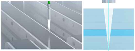 Figure 3. Multi-layer thickness measurements can be performed on display glass that has layers of transparent films with air gaps. Source: Micro-Epsilon
Conclusion
Using SLDs and innovative signal processing, white light interferometers enable absolute distance and thickness measurements with a high signal stability. This is ideal for industrial metrology use cases ranging from machine building to laboratory research and development, including applications in the semiconductor sector. Micro-Epsilon’s white light interferometers are specially designed to withstand these industrial environments and allow end users to rapidly align and set up their specific industrial metrology end application.