
Since 1995, imec and TEL have partnered to drive advances in patterning, logic, memory, and 3D integration. Their long-standing collaboration has led to key breakthroughs in areas such as High NA EUV lithography, etching, wet processing and deposition.
A standout achievement was the joint development of EUV resist coating track technology, which – thanks to its significantly improved defectivity control – has played a pivotal role in enabling the introduction of EUV technology into production.
Building on this foundation, the renewed partnership will focus on co-developing tools and process technologies to support the next wave of semiconductor scaling. Joint efforts will target High NA patterning technologies, aiming to boost performance through optimized material systems and improved defectivity control, as well as advanced deposition and etch solutions for next-generation CFET devices.
The agreement also reflects a shared commitment to sustainability, with imec and TEL continuing to explore environmentally responsible manufacturing processes for future semiconductor nodes.
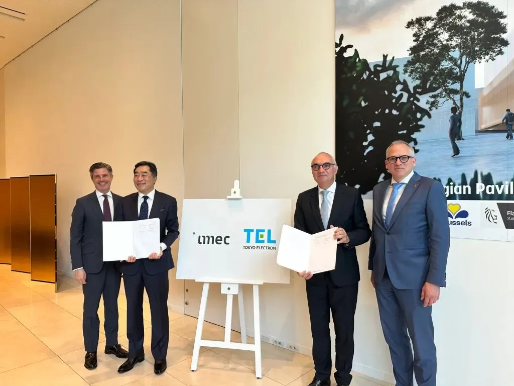
“This extended collaboration is another strong example of imec’s commitment to building international R&D partnerships that benefit the entire semiconductor ecosystem,” says imec CEO Luc Van den hove (pictured second from the right) “by deepening our alignment with TEL, we can garner valuable insights that will strengthen other flagship initiatives – such as the NanoIC pilot line under the European Chips Act. Hence, this partnership is truly a win-win: it reinforces TEL’s technology leadership while cementing imec’s position as a global hub for advanced semiconductor research – driving innovation well into the next decade.”