

In a forksheet device, the effective channel widths can be made larger than in a conventional gate-all-around nanosheet device due to a reduced spacing between n- and p-type transistors.
And this benefits the transistor’s drive current (or DC performance). In addition, the smaller n-to-p spacing enables a further reduction of the standard cell height, gradually pushing standard cells towards 4T track height design, meaning that 4 intracell metal lines fit in the range of the standard cell height.
But for 4T cell designs and metal pitches as tight as 16nm, even the forksheet becomes too narrow and struggles to deliver the required performance.
This challenge is highlighted in the 2022 VLSI paper by P. Schuddinck et al. [1]. And that’s where the complementary FET or CFET can provide relief.
Julien Ryckaert: “In a CFET architecture, n- and pMOS devices are stacked on top of each other. Stacking removes the n-p spacing from cell height considerations, allowing further maximization of the effective channel width, and, hence, the drive current. We can also use the resulting area gain to push track heights to 4T and below.”
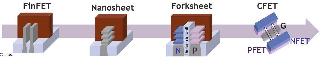
Figure 1 – From FinFET to nanosheet to forksheet and finally to CFET.
Two possible integration schemes are being explored for enabling the challenging nMOS-pMOS vertical stacking: monolithic versus sequential.
A monolithic CFET flow starts with the epitaxial growth of the bottom channel, followed by the deposition of an intermediate sacrificial layer, and next, the epitaxial growth of the top channel.
Naoto Horiguchi: “Although this seems the most straightforward way to build CFETs, the processing flow is rather complex. For example, the stacking approach results in very high aspect ratio vertical structures, which brings critical challenges for further patterning the fin, gate, spacers, and source/drain contacts.”
Imec develops modules and integration steps and quantifies the power-performance-area-cost (PPAC) benefits and the complexity of monolithic and sequential process flows.
Alternatively, CFETs can be made using a sequential fabrication flow consisting of several blocks. First, the bottom tier device is processed up to the contacts.
Next, a blanket semiconductor layer is created on top of this tier by wafer transfer, using a wafer-to-wafer bonding technique. Then, the top-tier device is integrated, and the top and bottom gates are connected.
Julien Ryckaert: “From an integration point of view, this flow is simpler than the monolithic flow, as both bottom and top-tier devices can be processed separately in a conventional ‘two-dimensional’ way. In addition, it offers the unique possibility of integrating different channel materials for n- and p-type devices.”
Each of these flows comes with its own set of pros and cons. Imec contributes by developing modules and integration steps and quantifying the power-performance-area-cost (PPAC) benefits and the complexity of each process flow.
In the paper, the authors present a PPAC evaluation of monolithic CFET vs. sequential CFET in a 4T standard cell design.
Julien Ryckaert: “From this benchmark, CFETs fabricated using a monolithic process flow are shown to consume less area and outperform their sequential counterparts, which suffer from a rise in effective capacitance. However, we show that we can put the trajectory of the sequential CFET on par with that of monolithic CFETs by applying three optimizations: (1) self-aligned gate merge ((v2) in the figure), (2) omission of the gate cap (v3), and (3) the use of hybrid orientation technology, referred to as HOT.”
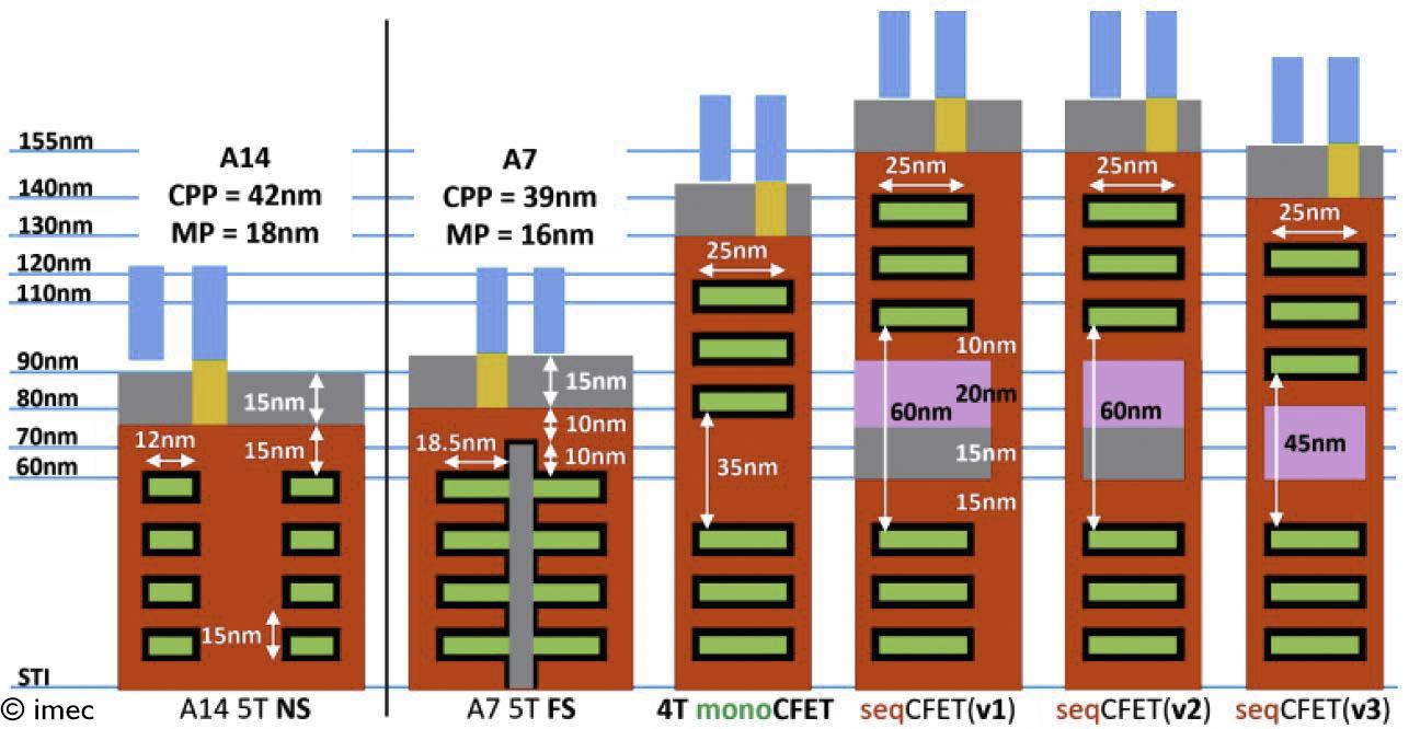
Figure 2 – Gate cross sections for nansoheet (NS), forksheet (FS) and CFET (monolithic and sequential). Basic sequential CFET (=v1) is wider and taller than mono. With an optimized flow (including self-aligned gate merge (v2) and no gate cap (v3)), sequential CFET approaches monolithic CFET in terms of area consumption (also presented at VLSI 2022).
HOT allows for independently optimizing the crystal orientation and strain engineering of top and bottom devices without adding to the process flow cost. For example, in an n-on-p configuration,
Si wafers with <100> orientation can be used on top, delivering the highest electron mobility for the top nMOS devices. While for the bottom, pMOS hole mobility benefits from the <110> Si wafer orientation.
Julien Ryckaert: “Although monolithic CFET remains the preferred choice, the uniqueness of the sequential process flow is that it can exploit this difference in wafer orientation.With these optimisations, our benchmark shows that the sequential CFET flow can be a valid alternative to the more complex monolithic CFET for future 4T track designs.”
In recent years, imec reported incremental progress in improving module and integration steps for monolithic and sequential CFETs.
At VLSI 2020, for example, imec was the first to demonstrate a monolithically integrated CFET architecture realized by optimizing critical module steps [2].
For sequential CFET, step-by-step improvements have been reported as well. Although bottom and top-tier devices can be processed separately in a conventional ‘two-dimensional’ way, the wafer transfer brings specific challenges.
For example, it comes with thermal budget constraints (to around 500°C or below) for both layer transfer and top-tier device processing to avoid any negative impact on the bottom-tier devices.
This is a concern for the gate-stack reliability of the top-tier device, which usually requires thermal steps of the order of 900°C. Earlier, imec demonstrated new approaches for maintaining good gate-stack reliability, including, among others, a low-temperature hydrogen plasma treatment for pMOS top devices.
Also, imec reported progress in the dielectric-to-dielectric wafer bonding step by developing a void-free thin bonding oxide process.
Imec evaluated three different processes for enabling layer transfer. Resesrchers studied the impact of the various process options on the device performance for both top (fully depleted silicon-on-insulator (FD-SOI)) and bottom (bulk FinFET) devices.
Naoto Horiguchi: “Especially promising from a cost perspective is SOITEC’s low-temperature Smart Cut flow, which uses an engineered bulk donor wafer to enable thin layer splitting at low temperature. The beauty of this approach is that it allows for reusing the donor wafer, making it a cost-effective solution. The other two approaches both rely on substrate removal by grinding and Si etch-back, which does not allow reuse of the donor wafer.”
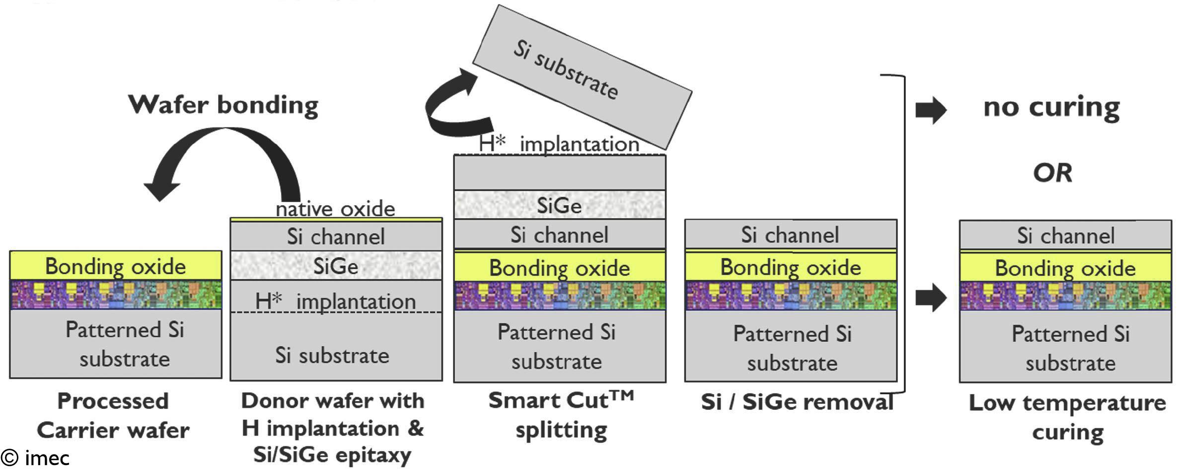
Figure 3 – Description of the SOITEC low-temperature Smart CutTM layer transfer flow, with no curing or low-temperature curing (also presented at 2022 VLSI).
With further optimisation, the top-tier devices processed after proof-of-concept layer transfer with low-temperature Smart Cut are shown to recover from degraded electrical performance.
Naoto Horiguchi: “The devices suffer from lower electron mobility due to the non-optimized low-temperature curing. Soitec has further developed its solution, showing that we can recover the mobility loss by optimizing the low-temperature curing step, which improves the crystal quality of the Si channel.
Given the cost-effectiveness of this approach, we consider Smart Cut with the newly developed process conditions a valid option for performing layer transfer in sequential CFET process flows.
It provides a generic flow enabling 3D sequential stacking applications beyond CFET, such as 3D sequential integration of memory-on-logic or logic-on-logic.”
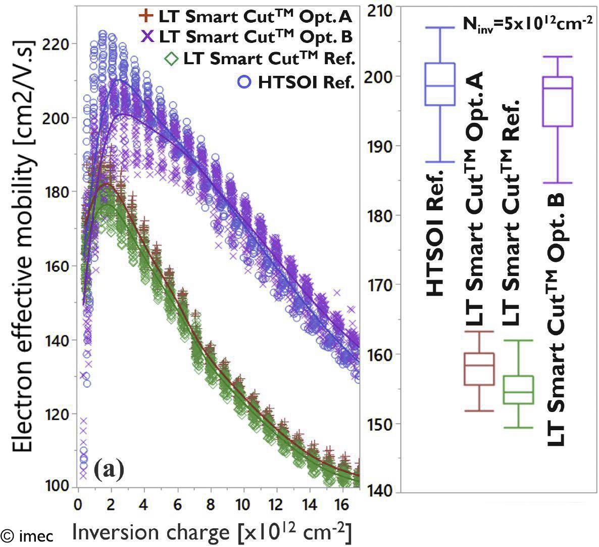
Figure 4 – Electron effective field mobility vs. inversion charge for the low-temperature Smart Cut layer transfer approach, comparing optimized and reference (proof-of-concept) process conditions. The graph shows improved mobility for Opt. B (purple), which refers to the additional low-temperature curing step (also presented at VLSI 2022).
With these test devices, the authors also showed good electrical interconnectivity between the top and bottom devices, validated through functional inverter chains. In addition, gate stack reliability of the top-tier pMOS devices was preserved by integrating the hydrogen plasma treatment step, as discussed above.
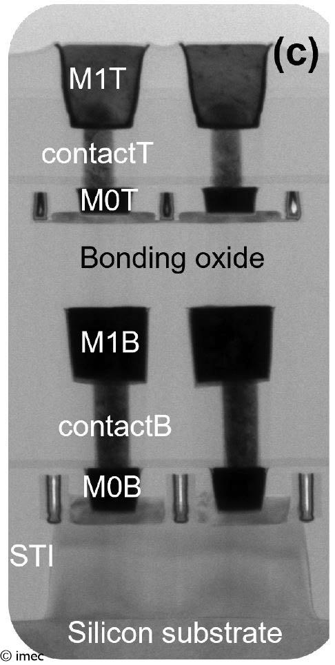
Figure 5 – TEM cross-section of the 3D sequentially stacked devices (also presented at VLSI 2022).
“I want to emphasize that this architecture is not yet a true CFET implementation,” adds Naoto Horiguchi. “For example, in the envisioned sequential CFET architecture, the metal interconnect layer (M1B) for the bottom device is absent.
Imec’s test vehicle was used to demonstrate improved layer transfer as a key module for sequential CFET and other 3D sequential stacking implementations. In the future, we continue to work towards optimized integration steps, which will eventually demonstrate a true sequential CFET implementation.