
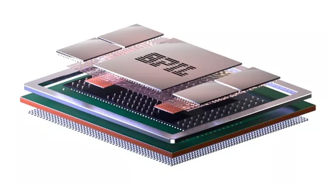
SPIL plans to deploy this differentiated capability across its 2.5D and fan-out package family technologies.
“Our challenge was to develop and deploy a proven advanced packaging assembly planning and verification workflow that included comprehensive 3D LVS,” says SPIL vp Dr. Yu Po Wang, “Siemens are a recognised leader in this space with a robust and proven workflow that we will use in production to validate our fan-out family of technologies.”
SPIL’s fan-out packaging family offers additional space for routing a higher number of I/O on top of the semiconductor’s area and extending the package size with a fan-out process, which cannot be achieved with conventional advanced packaging technologies