
Infineon has announced several new varieties of silicon and SiC MOSFETs for applications requiring robust switching. With trends toward decarbonization and improved efficiency in renewable energy, automotive, and industrial applications, the new MOSFETs can help designers reduce power waste and improve overall performance.

Each of Infineon’s newly announced MOSFETs features unique improvements targeting a variety of applications.
In this article, we’ll take a closer look at each of the new additions to Infineon’s MOSFET portfolio to learn more about the improvements compared to previous generations. We’ll also discuss the applications of each to give readers a sense of how designers can leverage the higher efficiency and power handling capabilities for next-generation devices.
Gen 2 SiC MOSFETs
First, Infineon recently announced its second-generation CoolSiC MOSFET series, which allows designers to boost efficiency and reduce size in high-power applications. Compared to silicon, SiC MOSFETs offer better power handling and thermal performance, paving the way for higher efficiency across the board.
This trend is continued with CoolSiC G2, with Infineon reporting voltage handling up to 1,200 V and a thermal resistance from case to junction as low as 0.19 K/W. As a result, designers can handle higher voltages and currents without having to resort to large form-factor switching devices.

Compared to previous generations, the CoolSiC G2 series enables smaller device sizes thanks to better thermal efficiency.
Taking an automotive use case as an example, Infineon has reported up to 10% power loss reduction using CoolSiC G2 while simultaneously increasing charging capacity and maintaining a familiar form factor. As a result, the CoolSiC G2 series could be useful in many applications, including renewable energy and DC-DC converters.
High-Voltage WBG MOSFETs
Infineon has also revealed new CoolSiC MOSFETs that push toward higher voltage handling capabilities. The new 2,000 V CoolSiC series provides higher voltage headrooms, allowing designers to leverage the FETs to increase the margin of safety compared to previous generations that break down at 1,700 V.
The CoolSiC 2,000 V series’ low on-resistance allows designers to handle large currents and voltages.
The 2,000 V series of CoolSiC MOSFETs (datasheet linked) can support up to 123 A of drain current, with a corresponding 12 mΩ on-resistance. Infineon specifically mentions 1,500 V DC link systems as a potential application. However, because of its breakdown voltages and currents, the 2,000 V series can be used in many applications, including fast EV charging and solar energy.
Improved Power Density With OptiMOS 6
Infineon also recently announced the OptiMOS 6 family of MOSFETs, which improves power density and reliability in smaller devices. As more applications turn to switching power supplies, the improvements offered by the OptiMOS 6 series (datasheet linked) allow designers to continue shrinking designs.
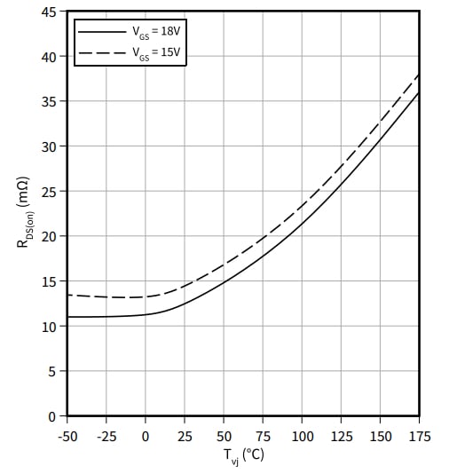
The power density of the OptiMOS 6 series creates a wide safe operating area.
Compared to the previous generation, OptiMOS 6 offers a 42% lower on-resistance and 89% lower reverse recovery charge, allowing designers to improve efficiency and EMI performance. In addition, the OptiMOS 6 can support voltages up to 200 V, which is critical for many applications. The OptiMOS 6 series targets a wide swath of use cases from e-scooters to compact server or telecom systems. The series is also useful for static switching applications, including battery management systems.
An Upward Trajectory of Improved Switching
Although not all designers will require the latest and greatest FETs, Infineon’s new offerings not only provide a wider range of MOSFETs to choose from but also push the boundaries of performance to reduce wasted energy. As more devices are electrified, Infineon’s upgraded MOSFET portfolio could be instrumental in keeping carbon footprints low for next-generation electronics.