
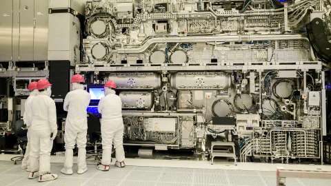
The $373 million machine, the size of a double decker bus and weighing over 150 metric tons, was transported to Oregon in more than 250 crates inside 43 freight containers. These were loaded onto multiple cargo planes that landed in Seattle. They were then transferred to 20 trucks for the drive to Oregon. The total weight of each new system is more than 150 metric tons.
“With the addition of High NA EUV, Intel will have the most well-rounded lithography toolbox in the industry, enabling the company to drive future process capabilities beyond Intel 18A into the second half of this decade,” says Mark Phillips, Intel Fellow and director of Lithography, Hardware and Solutions for Intel Foundry Logic Technology Development.
Intel plans to use the machine in the development of its 14A generation of chips in 2025, with early production expected in 2026 and full commercial production in 2027.
High NA EUV is expected to be able to print features up to 1.7x smaller than existing EUV tools. This will enable 2D feature scaling, resulting in up to 2.9x more density.
Compared to 0.33NA EUV, High NA EUV (or 0.55NA EUV) can deliver higher imaging contrast for similar features, which enables less light per exposure, thereby reducing the time required to print each layer and increasing wafer output.
Intel expects to use both 0.33NA EUV and 0.55NA EUV alongside other lithography processes in developing and manufacturing ICs, starting with product proof points on Intel 18A in 2025 and continuing into production of Intel 14A.
Intel’s approach will optimise process technology for cost and performance.
Although Intel co-founder Gordon Moore was an early proponent of the EUV concept, and Intel contributed several billion dollars to its development at ASML, Intel was late to use EUV tools in manufacturing preferring to use multi-patterning. This was a mistake which saw Intel slip behind the leaders in process technology.