
“The devices are designed to support applications requiring performance and power efficiency in low to mid-level storage capacities. They will also be integrated into Kioxia’s enterprise SSDs, in particular those that aim to maximise GPU efficiency in AI systems.” said the company.
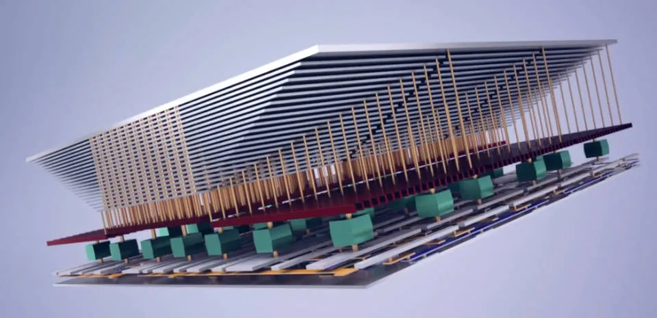
Production includes using wafer-level bonding to attach CMOS control die to the separately-fabbed memory stack – for the ninth generation this will be its state-of-the-art CMOS, with either a 112-layer memory from the company’s fifth generation, or a 218-layer 8th generation stack.
The flash being sampled has a 120-layer fifth-generation stack and “exhibits significant performance improvements over Kioxia’s existing flash products with the same 512Gb capacity – a sixth generation flash which is deploying the same 512Gbit triple-level cell as this product”, it said.
Claimed differnces are 61% improvement in write performance and a 12% improvement in read, and 36% write power efficiency and 27% in read.
Data transfer speed is 3.6Gbit/s (Toggle DDR6.0), with “up to 4.8Gbit/s under demonstration conditions” and “specifications of the samples may differ in mass production”, said Kioxia, adding: “ninth generation 3D flash memory will be suited for Internet of things devices and embedded systems in the industrial and automotive sector where cost and capacity are most important.”
It also pointed out that the memory figures above ids for devices before the subtraction of overhead data areas, formatting and bad blocks.
Last year, Kioxia started mass production of large quad-level cell flash memories
Image: representation of Kioxia’s 8th generation flash memory construction