
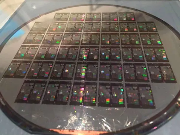
What has emerged from the research are narrow-band well-behaved lasers that are compatible with mass manufacturing.
“The lasers operate efficiently on a single O-band wavelength,” according to the IEEE Photonics Society, which has published the projects findings. “O-band is desirable as it allows for transmission of signals within photonic devices with low dispersion. The proposed integration technique can be applied to a variety of photonic integrated circuit designs, paving the way for a scalable monolithic integration of on-chip light sources for practical applications.”
Challenges for integrating lasers into silicon ICs include: growing low-defect III-V material, defining an effective laser structure and coupling light effectively into waveguides on the chip’s surface.
In this case, InAs quantum dots were selected as the laser gain medium because they are naturally tolerant crystal defects.
To minimise such defects, strain-engineered GaAs and InGaAs buffer layers were designed to minimise the effects of the differing silicon and InAs crystal lattices, and deposited by MOCVD.
On top of this, MBE deposition was picked to lay down alternating layers of AlGaAs optical cladding and quantum wells for the laser stack.
“These [quantum wells] are InAs dots inside an InGaAs matrix,” lead researcher Rosalyn Koscica told Electronics Weekly. “The InAs dots are formed spontaneously by the strain self-assembly process, using the Stranski-Krastanov layer-plus-island growth mode in MBE.”
The buffer stack would leave the laser stack high above the pre-formed silicon nitride optical waveguides on the wafer’s surface, so part of the scheme included etching 50μm wide and 4mm long trenches, or pockets – just deep enough to ‘loose’ the buffer layers – into the silicon surface before MOCVD.
These trenches have a second effect.
When the MOCVD and MBE epitaxial stacks are etched to define the lasers, they are left with sloping sides. If the stack is tall, these slopes mean that the waveguide can only start 5 to 15μm away from the end of the laser, according to the researchers, resulting in a long air gap and ~10dB of optical attenuation.
Having the buffer confined to a trench minimises the slope and allows the waveguide to start as close as 3μm from the laser end.
To further reduce attenuation due to the gap, the air within it was displaced by spinning a layer of the optical coupling material benzocyclobutene onto the chip.
Resulting coupling was good enough for two different techniques to be applied to promote narrow-band lasing: side-coupled silicon ring resonators, or distributed Bragg reflectors embossed into silicon nitride waveguides on each end of the 4mm laser.
As well as working and being compatible with standard chip making processes, the devices have proved reliable.
“Our integrated quantum dot lasers demonstrated lasing up to 105°C, and a [calculated] life span of 6.2 years while operating at 35°C,” said Koscica.
The work is published as ‘Quantum dot DBR lasers monolithically integrated on silicon photonics by in-pocket heteroepitaxy, in the IEEE Journal of Lightwave Technology.