
At the same time, the team revealed two other optically-active 2D parings: WSe2 – SnSe2, and black phosphorous with MoS2.
All the pairings are held in stacks by van der Waals force – the same force that hold graphene layers together in graphite – which pulls the layers together leaving a narrow gap across which the band structures of the opposing materials can interact.
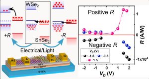
WSe2 – SnSe2
Stacked WSe2 and SnSe2, demonstrated the researchers, has an charge transport mechanism that can be controlled to have positive or negative photo responsivity, using light or an out-of-plane electric field,
Electric field dependent band-structure modelling in the project suggests this is due to the nature of band alignment at the interface, which changes from type-II alignment (thermionic transport) to type-III (tunnelling), and it is this that switches photocurrent activity from positive to negative.
With the switch to tunnelling comes a 10,000x is response speed (to ~1μs) and an increase in sensitivity, which can be turned on and off by transistor-like electric field biasing.
“In this study a high negative responsivity and fast response time was experimentally observed in the device prototypes which are encouraging for further development of 2D materials-based devices for practical applications,” according to Monash.
Black phosphorous with MoS2
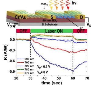 With other 2D pairing, black phosphorous and MoS2, the polarity of photoconduction showed a wavelength-dependence (graph left).
Negative photoconductance seen at chosen wavelengths above the absorption edge of MoS2 could be controllably and reversibly tuned to positive photoconductance at lower wavelengths.
MoS2 in this case was in flake form, and the wavelength at which positive behaviour swapped from positive to negative depended on the thickness of the flake, and could also be affected by transistor-like electrostatic gating or laser illumination.
“Thickness-dependent band-structure calculations carried by researchers from Monash clearly showed the possibility of an increase in recombination of charge carriers for specific thicknesses which could lead to negative photoconductance,” according to the university.
The team moots practical applications in broadband photo-detection and potentially multi-level optoelectronic logic or memory.
‘Polarity-tunable photocurrent through band alignment engineering in a high-speed WSe2/SnSe2 diode with large negative responsivity‘ published in ACS Nano
‘Wavelength-controlled photocurrent polarity switching in BP-MoS heterostructure‘ published in Advanced Functional Materials