
Today, ST announced it will install a Panel-Level-Packaging (PLP) production line at its site in Tours, France.
The line is expected to be operational in Q3 2026.
The $60m investment adds a second PLP line to its existing line in Muar, Malaysia.
“The development of our PLP capabilities in Tours is aimed at advancing this innovative approach to chip packaging and test manufacturing technology, boosting efficiency and flexibility so it can be rolled out across a wide portfolio of applications,” says Fabio Gualandris, president of quality, manufacturing and technology at ST. “With our fab in Malta, ST has already demonstrated its capability to deliver high-performing chip packaging and test in Europe. As we reshape our global manufacturing footprint, this new initiative in Tours will expand our process, design and manufacturing innovation capabilities supporting the development of next-generation chips in Europe.”
A multidisciplinary team covering experts in automation, process engineering, data science and R&D will support the project.
ST said the Tours project will leverage synergies with local research centres, including CERTEM.
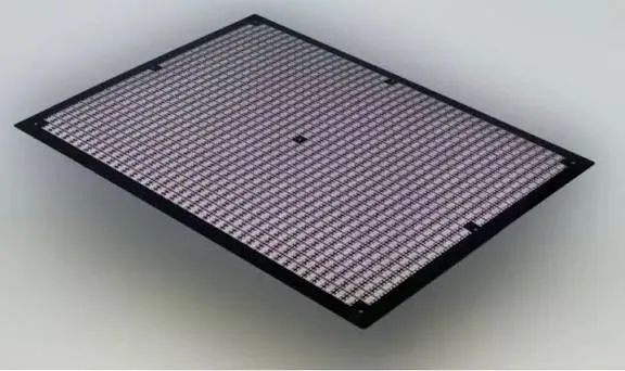
ST has been at the forefront of PLP development since 2020. The company’s R&D teams have worked to prototype and scale the technology, culminating in a state-of-the-art PLP process currently in production at volumes of over five million units per day on a highly automated line using very large, 700x700mm panels.
ST’s PLP technology focuses on Direct Copper Interconnect (DCI). Direct copper interconnections replace the traditional wire connections of chips with their encapsulation support.
DCI is the process by which these ICs are electrically connected to the panel substrate using copper, which is known for its excellent electrical conductivity.
DCI offers superior performance compared to traditional methods that use solder bumps, which can be less reliable.
This technology with direct connection without wire supports new product development by reducing power losses (such as resistance and inductance), enhancing heat dissipation and enabling miniaturisation. This leads to better overall power density.