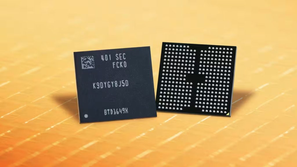
Compared with the 236-layer 8th gen memory, the 286-layer device increases bit density by 50%, data input and output speeds by 33% and reduces power consumption by 10%.
Innovations include cell interference avoidance and cell life extension and eliminating dummy channel holes has significantly reduced the planar area of the memory cells.

Samsung’s “channel hole etching” technology creates electron pathways by stacking mold layers and maximises fabrication productivity as it enables simultaneous drilling of the industry’s highest cell layer count in a double-stack structure.
As the number of cell layers increase, the ability to pierce through higher cell numbers becomes essential, demanding more sophisticated etching techniques.
The 9th-generation V-NAND is equipped with the Toggle 5.1 interface which supports increased data input/output speeds by 33% to up to 3.2 Gbps.
