
Until recently, a very common problem faced by electronic circuit designers was the difference in supply voltage standards between microcontrollers (e.g. 3.3 V) and peripheral ICs (e.g. 5 V). In order for them to operate together, the use of additional voltage translators was required, which made the device more complicated and increased the final price. Now, this is a thing of the past.
Microchip, a company that is known for its broad portfolio of 8-bit microcontrollers from the PIC® and AVR® families, continues to expand its assortmentrange. The newly developed ICs combine the best features of both product groups, offering to electronic designers a wide range of possibilities and making it easier to develop circuits that are even more integrated. This is the case with the energy-efficient, 8-bit microcontrollers from the AVR®DD/DB families. They feature a unique set of peripherals that operate independently from the core (CIP, Core Independent Peripherals), primarily for efficient analogue signal processing. They also ensure safe operation of applications in compliance with the IEC61508 and ISO26262 standards. Thanks to them, the AVR®DD/DB microcontrollers are perfectly suited for the needs of simple applications. They can also serve as companion (support) chips in more complex projects.
In this article, we discuss topics such as:
- The design of AVR® DB and DD microcontrollers
- The advantages and applications of the MVIO integrated voltage translator
- Prototyping and learning with the Curiosity Nano kits
- Clock signal supervisor IC
- The EVSYS and direct communication between the peripherals
- The advantages and capabilities of the built-in Custom Logic circuit
- Operational amplifiers in AVR®DB microcontrollers
- The operation of a core-independent ADC converter
General information about the AVR® DB and AVR® DD microcontrollers
The microcontrollers presented here have been designed to speed up and facilitate the design phase, thanks to which the production of the target device can be implemented quickly. Microchip accomplished this goal by integrating the AVR core with a range of peripherals in a single structure, allowing it to perform many tasks that previously had to be handled by external circuits. What’s more, the DB and DD products are available in a range of formats, from the classic DIPs to VQFN packages with a footprint of only 5×5 mm. This satisfies the needs of modern electronic circuits, such as remote IoT devices or programmable controllers, relays and industrial sensors.
To begin with, it should be noted that the ICs presented here have all typical features and functions of the Microchip products. They are clocked at 24 MHz, offer up to 128 kB of Flash memory (software memory), 16 kB of SRAM (operational memory) and 512 B of non–volatile EEPROM, traditionally used to store data on setpoints, serial numbers etc. The enclosures of the microcontrollers are fitted with up to 64 pins with diverse functionalities. Apart from the traditional role of the I/O ports (i.e. GPIO), they have been combined with ADCs and SPI, I2C, UART serial interfaces. A real-time clock (RTC), counters/timers (used, among other things, for generating PWM signals), analogue comparator and reference voltage sources (with several values) have also been integrated with the microcontrollers. In addition, the chip includes a digital-to-analogue converter (DAC) and an advanced watchdog. Other, more advanced components operating independently from the core (CIPs) have been discussed in detail later in the text.
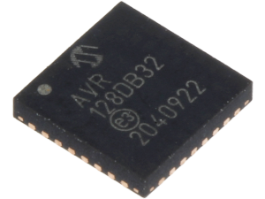
AVR128DB32-I-RXB
AVR® DB microcontrollers
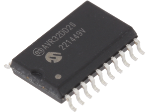
AVR32DD20-ISO
AVR® DD microcontrollers
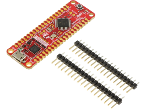
EV72Y42A
Development kits
Functionalities of MVIO
MVIO (Multi-Voltage Input/Output) is a configurable, integrated logic level voltage translator (level shifter). Thanks to it, some of the microcontroller’s leads can be supplied from a source with a different voltage value than the one supplying the unit’s core. Such a solution greatly improves and expands the capabilities of the microcontroller, as it enables safe communication of the microcontroller with the circuits using other logic levels (e.g. 5 V when supplied with 3.3 V). This means that designers can select the target circuit components freely, without worrying that the differences in electrical characteristics will result in a need to include additional intermediary circuits on the PCB.
The MVIO system has been designed to work with logic (digital) signals. Of course, its functionality includes both binary signals and hardware communication buses (e.g. SPI, I2C) or on-chip PWM controllers. Another advantage of having direct control over external components is that it is fully supervised by the microcontroller. If the MVIO’s supply voltage value (VDDIO2) drops below the pre-set value, an interrupt can be generated, to enable detailed monitoring of the device status. MVIO accepts voltages from 1.6 V to 5.5 V DC. In the event of a complete power failure on the VDDIO2 line, MVIO pins operate as tri-state inputs/outputs.
The MVIO peripheral can be easily configured in the MPLAB X and ATMEL STUDIO 7 development environments.
Development Kits
You can get acquainted with the functionalities of the AVR® DB and AVR® DD integrated circuits easily thanks to the development kits designed by the manufacturer. They have been made in the form of small PCBs with leads for mounting pin headers or for surface-mount technology (SMT) installation. Two boards can be purchased from the TME catalogue: EV72Y42 with the AVR64DD32 microcontroller and EV35L43A with the AVR128DB48 microcontroller.
Both belong to the Curiosity Nano family developed by Microchip. It is a platform aimed at efficient and gradual introduction of electronic engineers to concepts related to the programming and application of the AVR microcontrollers in products and individual projects. In terms of the kit contents, both models have a similar design. They use Micro USB sockets for communication with a PC and as the main power source. They feature signalling LEDs (software-operated, intended for indicating power supply status), quartz resonators clocking the core, a real-time clock (RTC) placed inside the microcontroller and a microswitch (connected to an I/O pin). Most importantly, though, the circuit includes an integrated debugger for detailed analysis of the microcontroller’s operation. In connection with the MVIO’s functionality, there are also separate leads for connecting alternative power supply voltage on the boards.
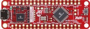
A small PCB comprises a complete AVR® DD series development kit.
Other capabilities of the DB and DD family ICs
Apart from the MVIO system, a number of other solutions is available in the microcontrollers presented here. These include CIPs, i.e. peripherals that operate independently from the core. The most important of these are listed below, although it should be noted that the full functionality of the AVR® DB/DD series is a very broad topic, and ICs may differ in design from model to model.
CFD (Clock Failure Detect)
CFD (Clock Failure Detect) – extremely important in terms of ensuring safe operation of the application. It is a circuit for monitoring the presence of a clock signal coming from an external oscillator (a quartz generator). If the signal disappears, the microcontroller will automatically switch to using an internally generated clock signal. At the same time, an interrupt will be triggered, which the designer can use in the application, for instance to stop the program or enter the safe mode to ensure secure and continuous operation of the IC.
EVSYS (Event System)
EVSYS (Event System) – a system that allows integrated peripherals to transmit signals directly to one another, independently from the core. Through EVSYS, an output from a single component can be passed to many other peripheral components. This improves the response time and reduces power consumption, while also allowing for the execution of more complex tasks, as the CPU core is not burdened with the need to constantly handle simple cyclic operations (e.g. conditional operations performed to monitor I/O ports).
CCL (Custom Logic)
CCL (Custom Logic) is only used in the AVR® DD family products. It is a set of embedded, programmable logic gates and flip-flops. With configurable connections, their inputs and outputs can be connected to the physical leads (pins) of the microcontroller. Alternatively, the design allows CCLs to be directly connected to on-chip integrated peripherals, as well as for the microcontroller software to read the CCL output states (although the operation itself remains independent from the core). In many cases, this will eliminate external logic circuits, and thus minimise the development cost of the device and the PCB size.
Integrated operational amplifier
An integrated operational amplifier (3 pcs) has been placed in the ICs from the AVR®DB group. Thanks to these mixed circuits, the microcontroller can perform the functions of an analogue signal analyser and a converter, and in this way reduce the number of external components required for this purpose. The latter can be limited to multiplexers or resistor ladders (if necessary).
Built-in analogue-to-digital converter (ADC)
Normally, the ICs from both of the families presented here have an integrated analogue-to-digital converter (ADC) with 12 bit resolution, characterised by a maximum sampling rate of 130 kS/s (thousands of samples per second). It uses a microcontroller-based reference voltage source featuring just a minimal temperature drift (low temperature coefficient) and providing values of 1.024 V, 2.048 V, 2.500 V and 4.096 V. Combined with the peripherals mentioned above, such as EVSYS and an internal comparator, the ADC allows for rapid, efficient and precise processing of analogue signals.
Text prepared by Transfer Multisort Elektronik Sp. z o.o.