
The end products have already been subject to product lifecycle management (PLM), pioneered by Siemens, which helps to trace and manage the entire lifecycle of a product from inception through design, realization, deployment, and field service, right through to end-of-life activities such as final disposal. That same level of scrutiny is now being adopted for the ICs that power those electronic products. The practice is known as silicon lifecycle management (fig 1).

Figure 1: Silicon lifecycle solutions encompass the complete cycle of design, realization, and utilization, addressing debug, test, yield management, safety and security, and in-field optimization.
Drivers and benefits of silicon lifecycle management
Progress in the semiconductor industry relies on process technology scaling, design scaling, and system-level scaling. Process technology scaling is the shrinking of circuitry, which leads to larger size and complexity of IC designs, which are built into devices that are ever more complex, pervasive, and mission-critical.
The challenges to staying competitive in the semiconductor markets of today and tomorrow span the entire IC lifecycle from conception to design, fabrication, and deployment. A solution lies in silicon lifecycle solutions (SLS) that give unprecedented visibility into the life of your silicon.
But what does SLS look like? An SLS platform collects data from the chip and from the processes involved in its production. It mines potentially huge volumes of data, delivering actionable information when and where it is needed. SLS establishes a holistic approach that allows semiconductor companies to improve existing processes. For example, advanced DFT techniques enhance IC quality, increase test efficiency, and enable diagnosis-driven yield analysis (DDYA). But SLS takes it further by using the on-chip hardware and DFT logic to monitor and asses circuit behavior and collect the data that feeds the fab-to-field optimization loop.
Embedded functional monitors are another key component of SLS. They acquire relevant data in a manageable form and then formulate and implement a local response where necessary. For example, the semiconductors used in the next generation of safety-critical devices deployed in cars must ensure reliability, safety, and security from cyber attacks. SLS is the framework through which an automotive SoC can be monitored and assessed throughout its entire service life.
Elements of silicon lifecycle management
SLS encompasses the traditional semiconductor value chain – design, manufacturing, test, and bring-up. It also reaches deep into the deployment phase of the device; providing information that makes it easier for customers to design-in the device and bring up end products, enabling continuous in-field monitoring for preventive maintenance in the field, and ensuring devices remain performant after field upgrades. It feeds information forward from the device manufacturer to OEM customers and end-users and takes information back from the field to the semiconductor conception and production process.
To realize the benefits of SLS, two elements are fundamental:
- The semiconductor architect needs to include design augmentations that gather data from the chip and facilitate the rest of the process.
- SLS must be recognized as a multi-actor paradigm that draws together semiconductor IP providers, chip developers, fabrication facilities (often external to the company developing the device), OEMs, service companies, and database and analytics providers.
At the “front end” of the process, the on-chip data sources include DFT logic, parametric monitors, and functional monitors. All the sensors, monitors, and DFT logic can produce huge amounts of data – enough to overwhelm even the best-designed analytics capability. A best-in-class monitoring infrastructure takes account of this by making monitors configurable at runtime to acquire only data of interest, by incorporating data compression technology, and including fast external connectivity to move the data off-chip.
As an example of a complete SLS platform, the Siemens Digital Industries Software (Siemens EDA) portfolio of tools that span the entire semiconductor value chain is illustrated in figure 2.
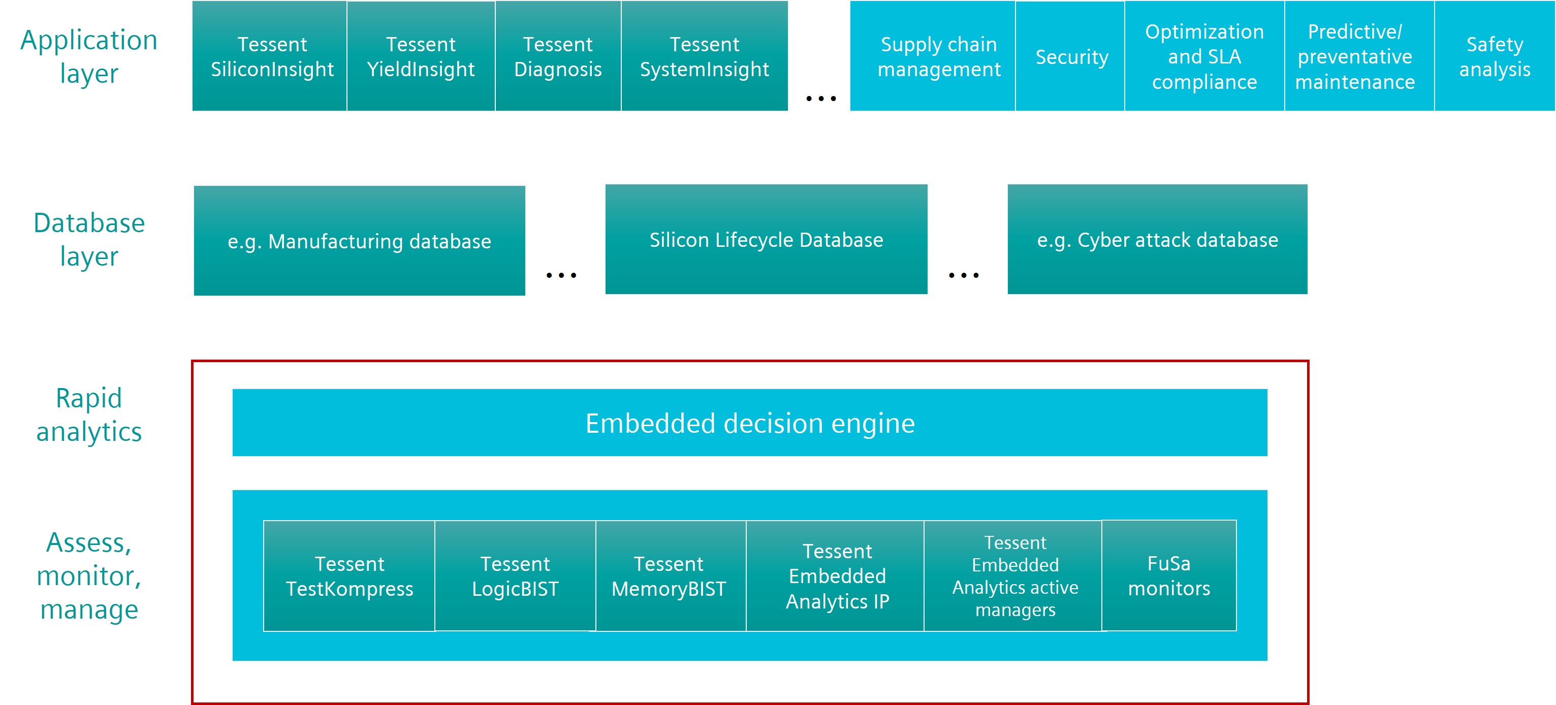
Figure 2: A high-level conceptual illustration of the Tessent Silicon Lifecycle Solutions platform.
This platform has four distinct layers:
Assess, monitor, and manage. This layer comprises the sensors and monitors that form the foundation of the SLS platform, gathering data about the system that can be used at various stages of the lifecycle. It includes the DFT logic that identifies structural defects and degradations, plus functional monitors (embedded analytics) that observe the interactions between silicon subsystems and between the silicon and the embedded software. These allow designers to intelligently monitor, understand and control the activity of any on-chip structure – including custom logic, interconnects, and CPU cores. These monitors provide full visibility into the silicon system, as well as smart data filtering and real-time, wire-speed operation.
Rapid analytics. This layer is a low-latency response embedded decision engine that detects, understands, and responds to a threat in the minimum amount of time. In some end-use applications, a fast reaction time is critical – in particular where there are security, safety, and privacy concerns such as in transportation or data centers. For example, in self-driving automotive applications, the system could detect stuck pixels on the camera feed and let the main CPU decide what course of action to take.
Database layer. The third layer comprises applications that gather and store the large amount of data generated by the on-chip monitoring IP at different stages of the lifecycle. This inevitably involves data from multiple vendors and sources – from design through manufacture, operation, and retirement. In recognition of this, open APIs, partnerships, federation capabilities, and participation in relevant standards organizations are critical factors for success.
Application layer. A host of applications can be enabled or enhanced by the use of data from silicon systems. Examples include applications for failure diagnosis, and root-cause analysis, test bring-up, debug, and silicon characterization, and system-wide debug in emulation and bring-up.
Many components of an SLS are ready and available, for example, the embedded IP for monitoring and analysis. One notable gap in the SLS flow until now has been how to export the chip data and use it in the enterprise software systems. Recently, a suite of software services addressing that need has been released. This software fills a key gap facing SLS early adopters—the need to extract data from SLS-enabled chips and use that data in existing flows and enterprise software systems and brings SLS one step closer to reality. This so called Host Services software is illustrated in figure 3.
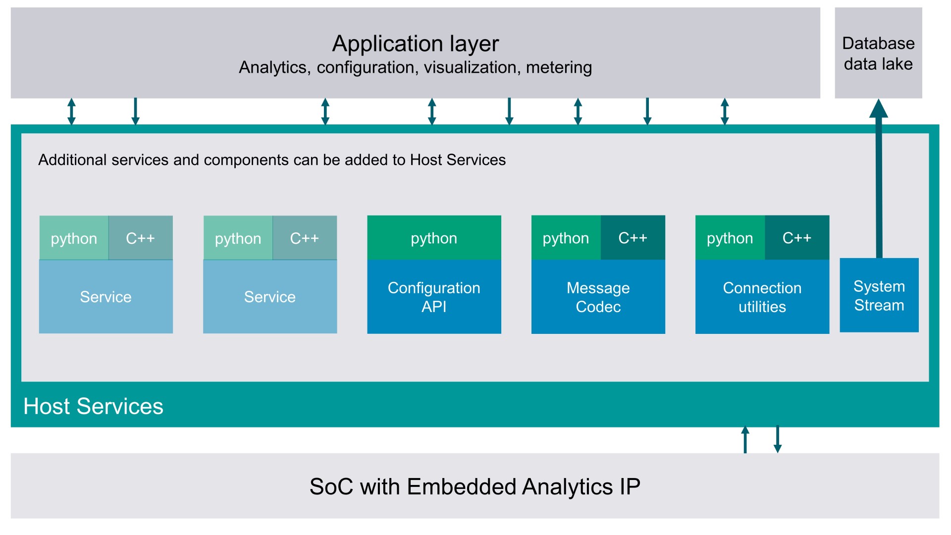
Figure 3. Host Services software opens the lines of communications to your SoCs, freeing the valuable data for multiple uses from system validation, testing, or continuous development and integration.
In sum, an SLS platform includes functional, structural, and parametric monitoring, analytics hardware and software (both on-chip and in the cloud), and a commitment to open interfaces, partnerships, federation capabilities, and appropriate standards efforts. SLS addresses the emerging and pressing need to apply product lifecycle management principles to the semiconductor value chain. Bringing together the silicon lifecycle management ecosystem will enable a new phase of growth and development in semiconductors, and allow the industry to keep its place at the heart of innovation for the next generation of products and technology.
Author – Aileen Ryan, Siemens EDA

Aileen Ryan is the senior director of strategy for Tessent Silicon Lifecycle Solutions, Siemens Digital Industries Software.