
A bipolar junction transistor (BJT) can function as either a small-signal amplifier or a switch. Though you don’t see many discrete BJT amplifiers on circuit boards these days—it’s vastly more convenient and effective to use an operational amplifier—it’s still common to encounter BJTs connected as switches.
BJT switches are typically used to block or deliver current to loads like brushed DC motors, lamps, or solenoids. They also sometimes appear in higher-frequency switching applications such as switch-mode regulators or Class D amplifiers. Figure 1 shows two common applications for a BJT switch: high-intensity LED illumination (left) and relay control (right). Both switches are actuated by a general-purpose input/output pin on a microcontroller.

Figure 1. Two examples of BJTs functioning as switches.
When designing BJT switch circuits, our focus tends to be on the currents and voltages we need to properly control the transistor and drive the load. However, it’s also important to consider power dissipation, especially in battery-powered or high-ambient-temperature applications. If we don’t, the BJT’s losses may increase component temperatures to the point of impaired performance or even thermal failure. At the very least, power dissipation will reduce the switch’s efficiency.
In this article, we’ll concern ourselves with two primary types of power dissipation: conduction loss and transition loss.
BJT Conduction Loss
As a switch, a BJT always operates in one of two modes:
- Fully off. No load current can flow and power dissipation is essentially zero.
- Fully on. Load current flows freely and power dissipation is low but non-zero.
In the on-state, the load current flows from the BJT’s collector to its emitter. A base-to-emitter current is also required to make collector-to-emitter conduction possible. The total power dissipation of these two current paths is known as the conduction loss (PC). We can calculate it using the following formula:
$$P_C~=~left(V_{BE}~times~ I_Bright)~+~left(V_{CE}~times~ I_Cright)$$
where:
VBE is the voltage across the base-to-emitter junction
VCE is the voltage across the collector-to-emitter junction
IB is the base current
IC is the collector current.
During conduction, VBE is usually around 700 mV. When the BJT is in saturation, which is the preferred mode for switching applications, VCE is around 200 mV. We can obtain a rough estimate of the conduction loss by assuming these fixed values, then determining base and collector current through standard circuit analysis techniques.
Using LTspice to Estimate Conduction Loss
SPICE simulations provide another, more accurate way of estimating conduction loss. Consider the LTspice circuit in Figure 2, for example. Q1 of this simulated bipolar junction transistor is controlled by a 3.3 V digital signal and switches current to a 50 Ω load.

Figure 2. A bipolar junction transistor modeled in LTspice.
Figure 3 shows the base-to-emitter and collector-to-emitter voltages that result when we run the simulation.

Figure 3. Base-to-emitter voltage and collector-to-emitter voltage during the active portion of the switching cycle.
The LTspice plot shows a VCE of 208.5 mV, which is very close to the 200 mV value we assumed in the preceding section. By contrast, VBE is significantly higher than we assumed—934 mV instead of the expected 700 mV.
We could insert these new values into our circuit-analysis calculations and generate a new estimate for conduction loss, but it’s much easier to let LTspice do the math for us. Just hold down the Alt key—or the Command key, if you’re using a Mac—and click on the transistor; LTspice will generate a plot like the one in Figure 4.
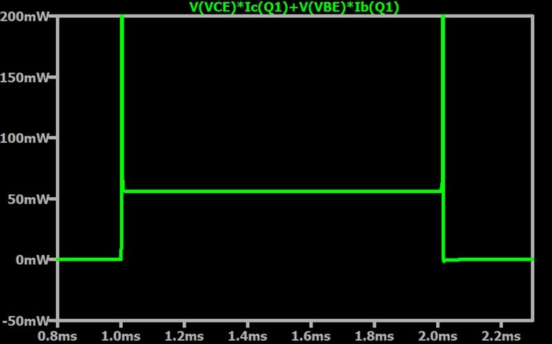
Figure 4. Transistor power consumption calculated and plotted by LTspice.
The results indicate that this BJT switch will dissipate a consistent 56 mW of power during the active phase of the switching cycle.
BJT Transition Loss
Those ominous spikes in the power-consumption plot above suggest that conduction loss isn’t the only type of power dissipation that we need to discuss. Figure 5 shows what happens if we zoom in on one of those spikes.
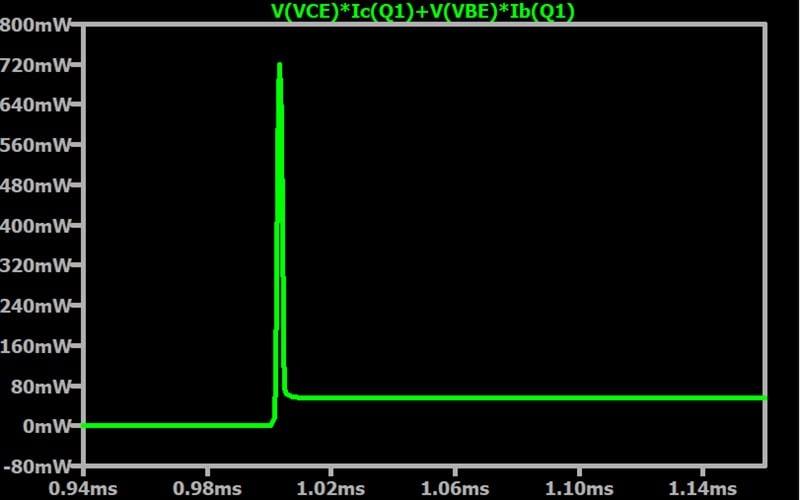
Figure 5. BJT power dissipation during the transition from the non-conducting cutoff state to the saturated conducting state.
These spikes occur because a BJT can’t change instantaneously from a non-conducting state to a fully conducting state. During the transition, significant collector current is flowing, and the collector-to-emitter voltage hasn’t yet settled into its low saturation level. Power dissipation is therefore relatively high.
You can see these current–voltage dynamics in Figure 6. The orange and red curves plot collector voltage and collector current, respectively; the green curve plots power dissipation.
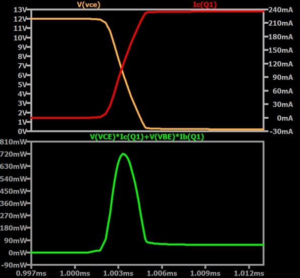
Figure 6. Collector voltage, collector current, and total BJT power dissipation during the transition from the switch-off state to the switch-on state.
There’s no straightforward way to accurately calculate transition losses. Multiple variables are involved, and the BJT’s currents and voltages change in rather complex ways. I suggest using simulations.
Let’s look at an example. Starting with the plot above, I can hold down the Ctrl key and click on the waveform label to perform integration (Figure 7). The area under the power curve represents energy loss, and this energy can be added up and divided by time to produce the average power dissipation due to BJT transition.
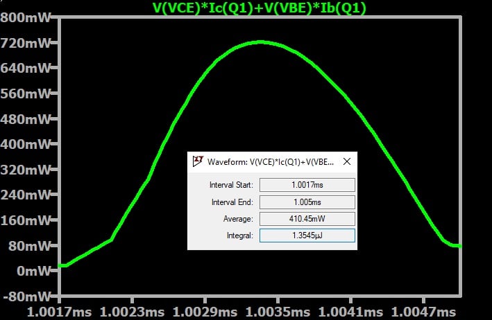
Figure 7. Integrating an instantaneous-power waveform with LTspice.
This indicates that each transition causes about 1.35 μJ of energy loss. Let’s say we’re switching at 500 Hz, or five hundred cycles per second, which corresponds to one thousand transitions per second. The total energy loss per second will be 1.35 μJ × 1000 = 1.35 mJ. The average power dissipation due to transitions is therefore 1.35 mW.
Even in situations where you don’t need a numerical estimate, you should be mindful of the following two parameters:
- Switching frequency. A higher switching frequency means more transitions per second and therefore higher time-averaged loss.
- Rise/fall times. Longer rise or fall times create more energy loss per transition.
Both of these factors strongly influence transition losses. For example, Figure 8 demonstrates that increasing the control signal’s rise time from 10 μs (the value used for the above simulation) to 100 μs raises the energy loss from 1.35 μJ to 13.7 μJ.
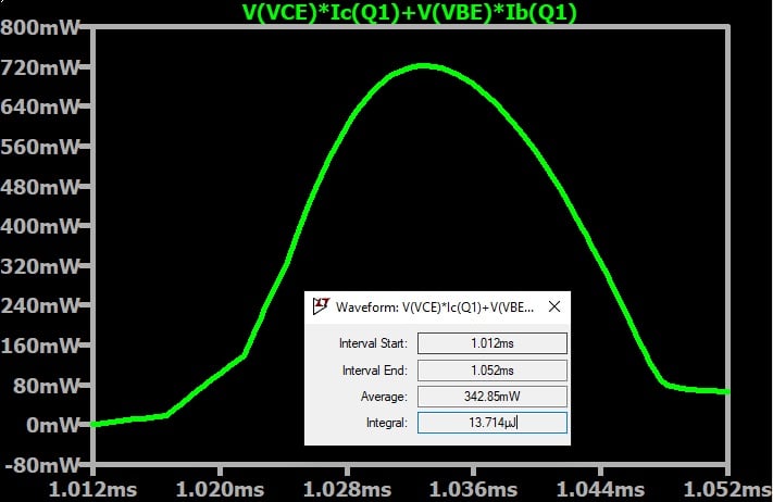
Figure 8. Slower transitions between on and off states lead to more energy loss.
Wrapping Up
As we saw in this article, SPICE simulation is a valuable tool for analyzing and predicting BJT switching losses. Understanding these sources of power dissipation can help designers to optimize their circuits and ensure that components aren’t stressed or damaged by excessively high temperatures.
All images used courtesy of Robert Keim