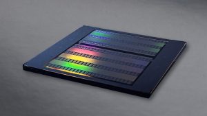
 The new name is a combination of technology and ascend, said the company’s press release, a sign, it says, of its commitment to develop its technical capabilities and to grow as a photomask provider. The company’s new logo depicts a photomask over a semiconductor wafer.
All of the company’s across the group will change, including Texmic Photomask Company in Shanghai, to Tekscend Photomask. The company’s headquarters are in Tokyo, Japan and there are eight manufacturing facilities in Taiwan, Germany, France, Korea, Singapore and two each in China and the US.
Earlier this year, the company signed a joint R&D agreement with IBM for a 2nm logic semiconductor node using ultraviolet lithography (EUV) The agreement also includes High-NA EUV photomask development capability on next-generation semiconductors. This photomask capability will be developed over five years at the Albany NanoTech Complex in New York, USA and the photomask plant in Niiza, Japan.
